🧩 Zephyr SPI Notes for Nordic microcontrollers - Part 3

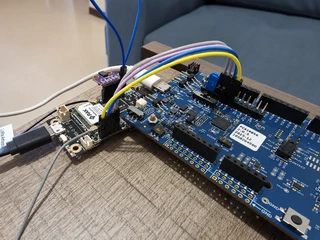 Image credit: [Me]
Once the SPI controller, pinctrl configuration, child nodes, and basic Zephyr API usage are in place, the next challenge is making the complete system reliable on real hardware.
A configuration may compile correctly and still fail because of an incorrect chip-select mapping, an unsuitable clock frequency, a floating MISO line, an unpowered peripheral, a missing binding, or a transaction that doesn’t match the device datasheet.
This final part focuses on that integration and debugging stage.
It covers how to choose a practical SPI frequency, manage several devices on the same bus, handle chip-select and interrupt GPIOs, create bindings for custom drivers, and integrate out-of-tree modules into a Zephyr workspace.
It also presents a layered debugging approach that moves from build configuration and runtime readiness to logic-analyzer captures, signal integrity, power sequencing, and incremental board bring-up.
The goal is not only to make one SPI transaction work. It is to understand where a failure begins, verify each layer independently, and build a communication path that remains reliable as more devices, interrupts, higher frequencies, and power-management features are added.
8. Frequency strategy
Each child device can define its own spi-max-frequency:
afe0 {
    spi-max-frequency = <24000000>;
};

flash@1 {
    spi-max-frequency = <83000000>;
};

acc@2 {
    spi-max-frequency = <4000000>;
};
The spi-max-frequency property belongs to the SPI child node because each device may support a different maximum SPI clock frequency.
However, this value is only one part of the decision.
The practical maximum SPI frequency is limited by:
1. The SPI peripheral’s specifications.
2. The capabilities of the selected nRF52840 SPIM instance.
3. The PCB layout and signal integrity.
4. The selected GPIO drive strength.
5. The voltage domain and loading on the bus.
6. The quality of CS, SCK, MOSI, and MISO waveforms.
A safe approach is to treat spi-max-frequency as an upper limit, not as the initial bring-up frequency. Don’t blindly copy the device’s maximum supported frequency from its datasheet into the devicetree.
For example, this is misleading on a typical nRF52840 SPIM bus:
flash: flash@1 {
    reg = <1>;
    spi-max-frequency = <83000000>;
};
Even if the flash memory itself supports a very high SPI clock, the nRF52840 SPIM controller and the board layout may impose lower limits.
A more conservative starting configuration would be:
flash: flash@1 {
    reg = <1>;
    spi-max-frequency = <1000000>;   # first bring-up
};
The frequency can then be increased gradually after obtaining reliable READ_ID and status-register responses.
A suggested bring-up sequence is:
| Stage | SPI frequency | Goal |
|---|---|---|
| First power-on | 500 kHz – 1 MHz | Verify wiring, CS behavior, and MISO activity |
| Identity reads stable | 1 – 4 MHz | Confirm that responses are repeatable |
| Functional tests | Device-dependent | Test register access, FIFO operation, and status reads |
| Optimization | Up to the device and layout limits | Increase speed only after confirming reliable operation and acceptable signal integrity |
9. Chip-select rules
In SPI, SCK, MOSI, and MISO are shared by all devices on the bus, but each device needs its own chip-select line.
SCK   -> shared
MOSI  -> shared
MISO  -> shared
CS0   -> accelerometer
CS1   -> flash memory
CS2   -> AFE
The chip-select line determines which SPI peripheral is active during a transaction.
Only one CS line should be active during a transaction.
Most SPI devices use an active-low chip-select signal:
CS high -> device not selected
CS low  -> device selected
Therefore, the devicetree configuration commonly uses:
GPIO_ACTIVE_LOW
For example:
cs-gpios = <&gpio0 17 GPIO_ACTIVE_LOW>;
Physical pull-up recommendation
On custom boards, adding a physical pull-up resistor to each CS line is often a good design practice.
The appropriate resistance depends on the connected device, the board design, and the recommendations in the device datasheet.
CS pull-ups help because:
- During reset, MCU pins may be high impedance.
- Before Zephyr configures GPIOs, CS may float.
- During power sequencing, a floating CS can accidentally select a device.
- A selected SPI device may drive MISO unexpectedly.
- Two selected devices can fight each other on MISO.
On custom boards,, CS pull-ups are more important than pull-ups on SCK, MOSI, or MISO.
A typical recommendation is:
CS lines       -> add external pull-ups, especially on custom boards
SCK / MOSI     -> usually no pull-up needed; driven by SPI master
MISO           -> usually no pull-up needed for normal operation
A weak pull on MISO can sometimes make idle logic-analyzer traces easier to read, but it isn’t normally required for SPI communication and shouldn’t be used to hide a real bus-contention problem.
Do not manually toggle CS unless you really need to
When using:
spi_write_dt()
spi_read_dt()
spi_transceive_dt()
with a valid spi_dt_spec, Zephyr can control the CS GPIO automatically for the transaction.
Therefore, avoid manually toggling CS around typical SPI calls:
gpio_pin_set_dt(&cs_gpio, 0);
spi_transceive_dt(&spi_dev, &tx, &rx);
gpio_pin_set_dt(&cs_gpio, 1);
That can conflict with the CS control already defined throughcs-gpios.
Manual CS control is an advanced case, useful only when a device protocol explicitly requires behavior that the SPI transaction API cannot express.
For most use cases, let Zephyr control CS through cs-gpios.
Common CS mistakes
Mistake 1: Wrong reg index
cs-gpios = <&gpio0 17 GPIO_ACTIVE_LOW>,
           <&gpio0 15 GPIO_ACTIVE_LOW>,
           <&gpio0 13 GPIO_ACTIVE_LOW>;

afe: optical-afe@0 {
    reg = <0>;  # Subtle mistake. Actually selects P0.17, not P0.13
};
If the device is wired to P0.13, then it should be:
afe: optical-afe@2 {
    reg = <2>;
};
Mistake 2: GPIO controller disabled
This is incomplete:
&spi3 {
    cs-gpios = <&gpio1 10 GPIO_ACTIVE_LOW>;
};
if &gpio1 is not enabled.
&gpio1 {
    status = "okay";
};
Mistake 3: CS pin also used by another peripheral
If the CS pin is already used by UART, I2C, PWM, NFC, buttons, LEDs, or another shield definition, SPI may compile but fail electrically.
Always compare:
- schematic
- PCB net names
- board .dts / .dtsi
- overlay file
- generated build/zephyr/zephyr.dts
10. Multiple SPI buses vs. multiple devices on one bus
There are two common ways to connect several SPI peripherals:
- Place multiple devices on the same SPI bus and assign a separate CS line to each one.
- Use separate SPI buses for devices with incompatible electrical, timing, or bandwidth requirements.
One bus, multiple CS lines
In this arrangement:
SCK, MOSI, MISO are shared.
Each device has its own CS line.
Only one device should be selected at a time.
This is usually best when:
- Devices share the same I/O voltage.
- Devices are physically close to the MCU.
- The total bandwidth requirement is reasonable.
- The layout is clean and trace lengths are controlled.
- The devices can tolerate the same electrical bus conditions.
- Software can safely switch frequency and mode per device.
This is a good default for boards that have several SPI peripherals, but they don’t all need to communicate continuously at max speed.
Separate SPI buses
A separate SPI bus can be useful when one device has special requirements.
This is preferable when:
- One device needs much higher throughput.
- One device is electrically noisy.
- One device is power-gated while others remain active.
- One device has strict timing or signal-integrity requirements.
- Devices require different modes and switching becomes risky.
- The PCB layout is cleaner with separate buses.
- Pin budget allows the separation.
11. Interrupt pins aren’t SPI pins
Some SPI devices expose extra pins such as:
INT
DRDY
RESET
BUSY
ENABLE
FIFO interrupt
These signals are not part of the SPI bus itself. They are handled as regular GPIOs.
For example, an AFE connected through SPI may also provide an interrupt output:
afe: optical-afe@2 {
    compatible = "manufacturer,reference";
    reg = <2>;
    spi-max-frequency = <10000000>;
    int1-gpios = <&gpio0 8 GPIO_ACTIVE_HIGH>;
};
In this configuration:
SPI communication still uses the SPI bus.
The interrupt signal uses GPIO P0.08.
Where interrupt properties belong
Interrupt GPIO properties normally belong in the child device node:
afe: optical-afe@2 {
    int1-gpios = <&gpio0 8 GPIO_ACTIVE_HIGH>;
};
They don’t belong in the SPI bus pinctrl group.
Correct:
&pinctrl {
    spi3_default: spi3_default {
        group1 {
            psels = <NRF_PSEL(SPIM_SCK,  0, 19)>,
                    <NRF_PSEL(SPIM_MOSI, 0, 21)>,
                    <NRF_PSEL(SPIM_MISO, 0, 23)>;
        };
    };
};
Incorrect:
&pinctrl {
    spi3_default: spi3_default {
        group1 {
            psels = <NRF_PSEL(SPIM_SCK,  0, 19)>,
                    <NRF_PSEL(SPIM_MOSI, 0, 21)>,
                    <NRF_PSEL(SPIM_MISO, 0, 23)>,
                    <NRF_PSEL(SPIM_INT,  0, 8)>;
        };
    };
};
The binding must define the property
If the child uses a generic compatible such as:
compatible = "vnd,spi-device";
then not every custom property is automatically valid.
A property such as:
int1-gpios = <&gpio0 8 GPIO_ACTIVE_HIGH>;
should be described in a binding if the node is intended to pass validation cleanly.
A custom binding should include:
properties:
  int1-gpios:
    type: phandle-array
    required: false
    description: Interrupt 1 GPIO
Application-level interrupt setup
In application code or driver code, the interrupt pin is usually handled with a gpio_dt_spec.
Example:
#define AFE_NODE DT_NODELABEL(afe)

static const struct gpio_dt_spec afe_int = GPIO_DT_SPEC_GET_OR(AFE_NODE, int1_gpios, {0});
static struct gpio_callback afe_int_cb;
static struct k_work afe_work;
A typical interrupt callback should stay short:
static void afe_gpio_callback(const struct device *port,
                                   struct gpio_callback *cb,
                                   gpio_port_pins_t pins){
    k_work_submit(&afe_work);
}
Then the work handler can perform heavier processing:
static void afe_work_handler(struct k_work *work){
    // Read status/FIFO over SPI here, outside the GPIO ISR context.
}
Why defer work?
Avoid performing long SPI transactions or heavy data processing directly inside a GPIO interrupt service routine.
A better pattern is:
GPIO interrupt triggers.
ISR submits k_work.
Work handler performs SPI read/status handling.
This keeps the interrupt routine short and moves the longer operation into thread context.
It also makes the application easier to maintain because interrupt detection and SPI processing remain separate responsibilities.
12. Bindings for custom drivers
A generic SPI child node can be enough when the application performs transactions directly through SPI_DT_SPEC_GET().
However, when the peripheral has its own reusable driver, custom GPIO properties, initialization procedure, or sensor API implementation, it is better to create a dedicated devicetree binding and driver.
An out-of-tree module could begin with this structure:
sensing_storage/
├── zephyr/ │
    └── module.yml
├── dts/
│   └── bindings/
│   └── sensor/
│   └── manufacturer,reference.yaml
├── drivers/
│   └── sensor/
│   └── reference/
│       ├── CMakeLists.txt
│       ├── Kconfig
│       └── reference.c
├── CMakeLists.txt
└── Kconfig
The binding describes the device properties that may appear in devicetree.
For example:
# dts/bindings/sensor/manufacturer,device.yaml

description: |
  Optical analog front end accessed through application-managed SPI transactions

compatible: "manufacturer,reference"

include: [sensor-device.yaml, spi-device.yaml]

properties:
  reg:
    required: true
  spi-max-frequency:
    type: int
    required: true
    description: Max SPI clock in Hz (up to 80000000)

  int1-gpios:
    type: phandle-array
    required: false
    description: Optional interrupt GPIO connected to the sensor’s INT1 pin

  reset-gpios:
    type: phandle-array
    required: false
    description: Optional reset GPIO
The important line is:
include: [sensor-device.yaml, spi-device.yaml]
That tells Zephyr this child is an SPI device and should accept normal SPI child properties such as:
reg
spi-max-frequency
Devicetree node after adding the binding
The device can then be represented in devicetree as:
afe: optical-afe@2 {
    compatible = "manufacturer,reference";
    reg = <2>;
    spi-max-frequency = <1000000>;
    int1-gpios = <&gpio0 8 GPIO_ACTIVE_HIGH>;
};
At this point, the node is no longer just a generic SPI connection. It is intended to represent a real SPI device.
However, a binding alone does not create a Zephyr device object.
Then, to use:
const struct device *dev = DEVICE_DT_GET(DT_NODELABEL(afe));
you also need a driver that creates the device object. That means:
Binding exists
-> Zephyr can validate the devicetree node and generate its metadata.

Driver is compiled
-> Driver initialization code is included in the firmware.

Driver creates the device object
-> DEVICE_DT_GET() can refer to that device.
Without that driver-created device object, the devicetree node may be valid while DEVICE_DT_GET() still produces a linker error.
Connecting the driver to Kconfig and CMake
The driver directory can contain a local Kconfig file:
config DEVICE3
    bool "Enable the reference optical AFE driver"
    depends on SPI
    depends on GPIO
    default n
    help
        Enables support for the reference optical analog front end.
Its CMakeLists.txt can add the driver source when the symbol is enabled:
zephyr_library()

zephyr_library_sources_ifdef(
    CONFIG_DEVICE3
    reference.c
)
The module’s top-level CMakeLists.txt can then include the driver directory:
add_subdirectory(drivers/sensor/reference)
Similarly, the module’s top-level Kconfig can include the driver configuration:
rsource "drivers/sensor/reference/Kconfig"
The exact organization can vary, but the purpose remains the same:
Kconfig decides whether the driver is enabled.
CMake decides which source files are compiled.
The driver source creates the Zephyr device object.
What zephyr/module.yml does
The zephyr/module.yml file tells Zephyr how the external repository participates in the build.
A minimal example is:
build:
  cmake: .
  kconfig: Kconfig

This means:

cmake: .
    -> Use the CMakeLists.txt file at the module root.

kconfig: Kconfig
    -> Include the Kconfig file at the module root.
The module can also contain devicetree bindings under dts/bindings. Once Zephyr recognizes the repository as a module, it can discover those bindings as part of the build.
Making the module visible to Zephyr
Creating the module files is not enough by itself. Zephyr must also know where the module repository is located.
There are two common approaches:
- Pass the local module path directly when building.
- Add the repository to the west workspace manifest.
The first option is convenient during early development. The second is more suitable when the module should become a reproducible part of the project workspace.
Option 1: Pass ZEPHYR_EXTRA_MODULES during build
For a local module outside the west workspace, build with:
west build -b smart_custom_board/nrf52840 app \
  -- -DZEPHYR_EXTRA_MODULES=/absolute/path/to/sensing_storage
This command can be read in two parts:
west build -b smart_custom_board/nrf52840 app
    -> Ask west to configure and build the application for the
       selected board.
--
    -> Stop processing west arguments. Everything after this marker
       is passed to CMake.

-DZEPHYR_EXTRA_MODULES=/absolute/path/to/sensing_storage
-> Tell the Zephyr build system to include this additional
    module directory.
In other words, west launches the build, but ZEPHYR_EXTRA_MODULES is a Zephyr CMake setting.
This approach is useful when:
- The module is still under development.
- The module exists only on the local computer.
- You want to test the module without changing west.yml.
- The module path differs between development environments.
If the build directory was previously configured without the module, perform a pristine build:
west build -p always -b smart_custom_board/nrf52840 app -- \
-DZEPHYR_EXTRA_MODULES=/absolute/path/to/sensing_storage
The -p always option forces west to recreate the build directory configuration, preventing old CMake state from hiding module changes.
One limitation is that an absolute local path is not portable. Another developer—or a continuous-integration server—may store the module somewhere else.
Option 2: Add the module to west.yml
For a module stored in its own Git repository, it can be added to the workspace manifest:
manifest:
    projects:
        - name: sensing-storage
          url: https://example.com/your-account/sensing-storage.git
          revision: main
          path: modules/sensing_storage
The fields mean:
name
    -> The project name used by west.

url
    -> The Git repository containing the module.

revision
    -> The branch, tag, or commit that west should check out.

path
    -> Where the repository will be placed inside the west workspace.
After updating the manifest, run:
west update
West then retrieves the repository and places it at the configured workspace path.
If that repository contains a valid zephyr/module.yml, Zephyr can recognize it as a module during the build.
A west project and a Zephyr module are related concepts, but they are not identical:
west project
    -> A Git repository managed by the west manifest.

Zephyr module
    -> A repository that provides Zephyr build content,
       commonly described through zephyr/module.yml.
A west project may contain tools, documentation, or other files and may not be a Zephyr module. Conversely, a local Zephyr module can be included through ZEPHYR_EXTRA_MODULES without being managed by west.yml.
Using west.yml is usually preferable when:
- Multiple developers need the same repository.
- The project is built in continuous integration.
- A specific module revision must be reproducible.
- Running west update should retrieve all required dependencies.
- The module is a long-term part of the product workspace.
13. Early debugging checklist
Debug SPI in layers. Don’t jump directly to rewriting the driver.Debug SPI in layers. Do not jump directly to rewriting the driver or changing the transaction code.
A layered approach helps determine whether the failure comes from.
Layer 1: build configuration
Check:
[ ] CONFIG_SPI=y
[ ] CONFIG_GPIO=y
[ ] CONFIG_PINCTRL=y
[ ] The intended SPI node has status = "okay"
[ ] The GPIO controller used for CS has status = "okay"
[ ] The pinctrl labels referenced by the SPI node exist
[ ] The child node compatible matches the intended access pattern
Useful generated files include:
build/zephyr/.config
build/zephyr/zephyr.dts
build/zephyr/include/generated/zephyr/devicetree_generated.h
Common build-time failures
| Symptom | Likely cause | Fix |
|---|---|---|
compatible "nordic,nrf-spim" not recognized | Wrong devicetree context, missing SoC include, or invalid board inheritance | Check board DTS, SoC DTSI, NCS version, and perform a pristine build |
__device_dts_ord_* link error | The C code requested a device object that no compiled driver created | Use SPI_DT_SPEC_GET() for an application-managed SPI child, or compile a real driver for that compatible |
| Child property rejected | Binding doesn’t allow that property | Add an appropriate custom binding or remove the unsupported property |
| SPI node disabled | status = "okay" missing or overridden | Inspect build/zephyr/zephyr.dts |
| Kconfig warning: symbol assigned but not used | Wrong symbol, unmet dependency, or an internal symbol was forced directly | Enable the public Zephyr feature and inspect its dependencies |
| CS GPIO not ready | The GPIO controller is disabled, the wrong port is referenced, or the CS entry is invalid | Check the GPIO controller status and the cs-gpios mapping |
| Pin conflict | The same GPIO is assigned to another peripheral or board function | Compare the schematic, DTS files, overlays, and generated devicetree |
When a build-time failure appears, avoid changing the SPI command code. The firmware has not yet reached the point where protocol behavior can be tested.
Layer 2: runtime readiness
Before the first transfer, check the spi_dt_spec:
if (!spi_is_ready_dt(&spi_dev)) {
    LOG_ERR("SPI device not ready");
    return -ENODEV;
}
This verifies that the SPI controller and any CS GPIO described by the spi_dt_spec are ready for use.
If the check fails, verify:
[ ] Is the SPI controller enabled?
[ ] Is the GPIO controller used for CS enabled?
[ ] Is the CS GPIO specification valid?
[ ] Does the child node's reg index match the intended cs-gpios entry?
[ ] Does the final generated devicetree match the expected overlay?
.
Identity and status checks
Similar to checking a known register on an I2C device, create one simple identity or status transaction for each SPI peripheral.
Examples:
| Device | Typical check |
|---|---|
| AFE | Read CHIP_ID, for example register 0x0008 |
| Accelerometer | Read device ID registers |
| SPI flash | Send READ ID, commonly opcode 0x9F, and compare manufacturer/device ID |
The exact command, frame length, dummy-byte requirements, and expected response must come from the peripheral datasheet.
A useful bring-up pattern is:
1. Access only one device.
2. Send its identity or status command.
3. Read the expected number of response bytes.
4. Extract the response from the correct RX offset.
5. Compare it with the expected value.
6. Repeat the transaction many times.
7. Continue with the next device only after the first one is stable.
The application can keep each check in a separate function:
ret = read_accel_id();
if (ret < 0) {
    LOG_ERR("Accelerometer ID read failed: %d", ret);
}

ret = read_flash_id();
if (ret < 0) {
    LOG_ERR("Flash ID read failed: %d", ret);
}

ret = read_afe_chip_id();
if (ret < 0) {
    LOG_ERR("AFE CHIP_ID read failed: %d", ret);
}
Each function should implement the command format required by its own device rather than relying on a generic identity-read transaction.
If the SPI specification is ready and the API call succeeds, verify that the transaction itself matches the peripheral datasheet.
Check:
[ ] Is the command opcode correct?
[ ] Are register addresses sent in the correct order?
[ ] Are read/write bits placed correctly?
[ ] Are all required header bytes included?
[ ] Are dummy bytes included only when the protocol requires them?
[ ] Is the RX response read from the correct offset?
[ ] Does CS remain active across the complete command and response?
[ ] Is the configured SPI mode correct?
A common mistake is to assume that a successful call means that the frame was correct. The SPI controller can successfully transmit a frame that the peripheral doesn’t understand.
Layer 3: electrical behavior
Use an oscilloscope or logic analyzer.
Check:
[ ] CS idles in its inactive state.
[ ] Only the intended CS line becomes active.
[ ] SCK toggles at the expected frequency.
[ ] MOSI carries the expected command bytes.
[ ] MISO changes when the selected peripheral should respond.
[ ] CS remains active for the complete transaction.
[ ] Inactive peripherals release MISO.
If the logic analyzer shows no activity, return to the configuration and runtime-readiness layers.
If the waveforms are present but the data is incorrect, investigate the SPI mode, command format, signal integrity, and peripheral state.
Runtime failure table
| Symptom | Likely cause | First steps |
|---|---|---|
spi_is_ready_dt() false | Bus or CS GPIO not ready | Inspect the final DTS, GPIO status, CS mapping, pinctrl, and Kconfig |
| Works at 1 MHz but not 8 MHz | Limits imposed by layout, on signal integrity and drive strength | Reduce the frequency and inspect the waveforms |
All reads return 0x00 or 0xFF | MISO is held low or floating, the device is unpowered, the wrong bytes are being inspected, or the protocol is incorrect | Check power, voltage levels, reset, transaction patterns, MISO waveform, SPI PCB layout |
| Identity value changes randomly | Frequency is too high, signal integrity is poor, CS timing is unstable, or MISO contention exists | Verify reg against cs-gpios and test devices individually |
| Only one device works | Incorrect CS mapping, another device is driving MISO, or one peripheral is affecting the shared bus | Check reg to cs-gpios mapping |
| Device works after reset only sometimes | Startup timing, power sequencing, reset timing, or incomplete rail discharge | Add proper startup delay and verify rails |
| Write appears to be ignored | Missing command bytes, an incomplete frame, write protection, or incorrect byte order | Compare exact SPI transaction frame with datasheet |
14. Logic analyzer / oscilloscope checks
A logic analyzer is one of the fastest tools for debugging SPI protocol problems. An oscilloscope becomes especially useful when the digital transaction appears correct but communication becomes unreliable at higher frequencies.
For each SPI device, capture at least:
CS
SCK
MOSI
MISO
When several devices share the bus, capturing all CS lines together can also reveal accidental device selection or MISO contention.
What a healthy transaction looks like
For a device with active-low chip select, a typical transaction follows this sequence:
1. CS starts high.
2. CS goes low and selects the device.
3. SCK begins toggling.
4. MOSI carries the command, address, or payload bytes.
5. MISO carries response data during the expected part of the frame.
6. SCK stops toggling.
7. CS returns high.
8. All other CS lines remain high throughout the transaction.
Basic checks
[ ] CS idles in its inactive state.
[ ] The target CS becomes active before SCK starts.
[ ] The target CS remains active for the complete transaction.
[ ] The target CS returns inactive after the final clock edge.
[ ] All other CS lines remain inactive.
[ ] The SCK frequency matches the configured value.
[ ] MOSI carries the expected command and address bytes.
[ ] MISO changes when the selected device is expected to respond.
Check command alignment
SPI is full-duplex. The controller receives one bit for every bit it transmits, even while it is sending command or address bytes.
For example, suppose a device expects a two-byte command followed by a two-byte response, and its protocol requires dummy bytes to generate the response clocks:
TX:  command0 command1 dummy0 dummy1
RX:  junk0    junk1    data0  data1
The first two received bytes may not contain useful data because they were captured while the command was being transmitted.
In this case, the application must read the response from the correct RX offset:
uint8_t response0 = rx_buf[2];
uint8_t response1 = rx_buf[3];
The exact offset depends on the peripheral’s transaction format. Some devices return data immediately, while others require address bytes, turnaround clocks, or dummy bytes before the response becomes valid.
Don’t assume that the first byte in the RX buffer is the first response byte. Compare the captured frame with the timing diagram in the device datasheet.
Check SPI mode
An incorrect CPOL or CPHA setting can produce responses that look shifted, unstable, or consistently incorrect.
On the logic analyzer, verify:
[ ] The SCK idle level matches the datasheet.
[ ] MOSI changes on the expected clock edge.
[ ] The peripheral samples MOSI on the correct edge.
[ ] MISO becomes valid before the controller's sampling edge.
[ ] Data is not shifted by one bit.
Check MISO contention
When several peripherals share the same SPI bus, only the selected device should drive MISO.
Possible symptoms of MISO contention include:
- distorted or intermediate MISO voltage levels
- unstable identity-register values
- one device working only when another device is disconnected
- responses depending on which device was accessed previously
- communication becoming reliable when the frequency is reduced
Capture the MISO signal together with every CS line.
Verify:
[ ] Only one CS line is active.
[ ] Inactive devices release MISO.
[ ] MISO returns to an idle or high-impedance state after CS becomes inactive.
[ ] No device continues driving MISO after its transaction finishes.
If two CS lines become active simultaneously, correct the CS mapping or GPIO behavior before investigating the command protocol.
Some devices don’t place MISO into a high-impedance state under every operating condition. This should be verified in each peripheral datasheet before placing multiple devices on the same bus.
Check power-gated devices
A powered-off peripheral may still affect the shared SPI bus through its I/O protection structures.
When a device is power-gated, verify:
[ ] It doesn't clamp SCK.
[ ] It doesn't clamp MOSI.
[ ] It doesn't drive or clamp MISO.
[ ] Its CS line remains inactive.
[ ] It isn't being back-powered through I/O pins.
Power-sequencing problems can look exactly like SPI protocol failures. Compare the SPI signals with the peripheral supply and reset signals when the problem occurs during startup or shutdown.
15. An example of a bring-up order for custom boards
The safest bring-up strategy is incremental.
Do not enable every SPI device, interrupt, FIFO, power-management feature, and high-speed transfer at the same time. Each additional feature introduces another possible source of failure.
Instead, begin with the smallest working configuration and add one new variable at a time.
Phase 1: Hardware sanity
[ ] Confirm that all required power rails are present and stable.
[ ] Confirm that the logic voltage is compatible with the nRF5 I/O levels.
[ ] Confirm the state of device power-enable pins, if present.
[ ] Confirm the state of reset pins, if present.
[ ] Wait for the device's required startup time.
[ ] Confirm that every CS line idles in its inactive state.
[ ] Confirm that the intended SPI signals reach the correct device pins.
Phase 2: Devicetree sanity
[ ] Enable the intended SPI controller node.
[ ] Define pinctrl for SCK, MOSI, and MISO.
[ ] Add the required CS GPIO to the controller's cs-gpios property.
[ ] Enable gpio0 or gpio1 as required.
[ ] Add only one SPI child node.
[ ] Verify that the child node's reg value selects the correct CS entry.
[ ] Set spi-max-frequency to 1 MHz or lower.
[ ] Perform a pristine build.
[ ] Inspect build/zephyr/zephyr.dts.
Phase 3: C-level readiness
[ ] Create one spi_dt_spec using SPI_DT_SPEC_GET().
[ ] Confirm that the selected SPI mode matches the datasheet.
[ ] Confirm that spi_is_ready_dt() returns true.
[ ] Log a clear message when the readiness check passes or fails.
Phase 4: First transaction
[ ] Send one known identity or status command.
[ ] Use the exact frame format described in the datasheet.
[ ] Keep CS active for the complete command and response.
[ ] Include dummy bytes only when the device protocol requires them.
[ ] Read the response from the correct RX offset.
[ ] Check the SPI API return value.
[ ] Repeat the transaction many times.
[ ] Capture CS, SCK, MOSI, and MISO.
Phase 5: Add devices one by one
After the first device is stable, add the remaining SPI peripherals individually. Confirm that identity reads and read status transactions are fine.
Phase 6: Functional tests
[ ] Write one simple configuration register.
[ ] Read the same register back when the device supports readback.
[ ] Configure the basic operating mode.
[ ] Read status registers.
[ ] Test one measurement or data-acquisition path.
[ ] Test FIFO operation if required.
[ ] Test interrupt behavior only after polling works.
Phase 7: Frequency optimization
[ ] Repeat identity reads.
[ ] Repeat register read/write tests.
[ ] Exercise the main data-transfer path.
[ ] Check for intermittent errors.
[ ] Inspect CS, SCK, MOSI, and MISO.
[ ] Check rise time, ringing, overshoot, and sampling margins when needed.
Phase 8: Power management testing
Test:
[ ] Device sleep and wake-up commands.
[ ] MCU sleep and resume behavior.
[ ] Power-gating and power restoration.
[ ] CS state while the device is powered off.
[ ] SPI pin states during low-power modes.
[ ] Startup delays after power restoration.
[ ] Device reinitialization after wake-up.
[ ] Possible back-powering through SPI or GPIO pins.
Phase 9: Production-driver structure
[ ] A device-specific devicetree binding.
[ ] Driver configuration and runtime data structures.
[ ] DEVICE_DT_DEFINE() or a subsystem-specific device macro.
[ ] Kconfig and CMake integration.
[ ] Initialization and readiness checks.
[ ] Concurrency protection for shared state or SPI access.
[ ] Error propagation and recovery.
[ ] Power-management support.
[ ] Automated tests for register and protocol handling.
16. Final checklist before blaming the driver
Use this checklist when the SPI peripheral is not responding and you feel tempted to rewrite the driver.
Work through each category systematically. A failure that appears to come from the driver may instead originate in the devicetree, build configuration, transaction format, PCB, power sequence, or signal integrity.
Devicetree
[ ] Is the intended SPI controller node enabled?
[ ] Are SCK, MOSI, and MISO defined in pinctrl configuration?
[ ] Are the correct pinctrl states referenced by the SPI controller?
[ ] Are the CS pins listed in the controller's cs-gpios property?
[ ] Does each child node use the correct reg index?
[ ] Does each child node's unit address match its reg value?
[ ] Does each spi-max-frequency value use a supported frequency?
[ ] Are gpio0 and gpio1 enabled as required?
[ ] Are interrupt, reset, enable, and busy pins described as GPIOs?
[ ] Does each child compatible match the intended access pattern?
[ ] Does the custom binding allow every property used by the child node?
[ ] Does build/zephyr/zephyr.dts match the schematic and PCB layout?
Kconfig / build
[ ] Is CONFIG_SPI=y enabled?
[ ] Is CONFIG_GPIO=y enabled when CS or auxiliary GPIOs are used?
[ ] Is CONFIG_PINCTRL=y enabled?
[ ] Are the required logging options enabled for debugging?
[ ] Are unnecessary low-level nrfx symbols avoided?
[ ] Is the expected SPI backend enabled in build/zephyr/.config?
[ ] Is the custom driver's Kconfig symbol enabled, if applicable?
[ ] Are all Kconfig dependencies satisfied?
[ ] Is the external Zephyr module included in the build, if applicable?
[ ] Does the build output confirm that the module was detected?
[ ] Was a pristine build performed after devicetree, binding, module, or Kconfig changes?
C access pattern
[ ] Are generic SPI children accessed with SPI_DT_SPEC_GET()?
[ ] Is DEVICE_DT_GET() used only for real driver-backed children?
[ ] Does the driver instantiate the device node when used?
[ ] Is spi_is_ready_dt() checked before transfers?
[ ] Are auxiliary GPIOs checked with gpio_is_ready_dt()?
[ ] Are operation flags correct for the device?
[ ] Is the response copied from the correct RX offset?
[ ] Are return values checked after every SPI call?
[ ] Are transport errors logged separately from unexpected device responses?
SPI protocol
[ ] Is the SPI mode correct?
[ ] Is the bit order correct?
[ ] Is the word size correct?
[ ] Is the configured frequency conservative enough for bring-up?
[ ] Is the command opcode correct?
[ ] Are register addresses transmitted in the required byte order?
[ ] Are read/write indicator bits placed correctly?
[ ] Are all required command and header bytes included?
[ ] Are dummy bytes included only when required by the peripheral?
[ ] Is the expected number of clock pulses generated?
[ ] Does CS remain active for the complete command and response?
[ ] Are command, response, and turnaround timing requirements respected?
[ ] Are writes transmitting the complete frame rather than only the data value?
[ ] Are write-protection, busy, or status conditions handled correctly?
Chip-select behavior
[ ] Does each CS line idle in its inactive state?
[ ] Is the active level consistent with the peripheral datasheet?
[ ] Is the correct CS selected for each child node?
[ ] Does only one CS line become active during a transaction?
[ ] Does CS become active before the first clock edge?
[ ] Does CS remain active until the final clock edge is complete?
[ ] Does CS return inactive after the transaction?
[ ] Are external CS pull-ups present where required?
[ ] Does CS remain inactive during MCU reset and peripheral power sequencing?
[ ] Is software avoiding unnecessary manual CS toggling?
Hardware and power
[ ] Is the peripheral powered at the expected voltage?
[ ] Are the MCU and peripheral logic levels compatible?
[ ] Are all required power rails stable?
[ ] Has the peripheral completed its specified startup time?
[ ] Is the peripheral released from reset?
[ ] Are enable or shutdown pins in the correct state?
[ ] Are the SPI signals connected to the intended package pins?
[ ] Does the PCB net mapping match the devicetree pin mapping?
[ ] Are the physical components correctly placed and soldered?
[ ] Are CS lines held inactive during reset?
[ ] Do inactive devices release MISO?
[ ] Are powered-off devices clamping the shared bus?
[ ] Is any peripheral being back-powered through SPI or GPIO pins?
[ ] Are decoupling and grounding adequate near the peripheral?
[ ] Are traces, connectors, branches, and stubs suitable for the selected frequency?
Shared bus behavior
[ ] Do all devices use compatible I/O voltages?
[ ] Does each device have a dedicated CS line?
[ ] Does each reg value select the intended cs-gpios entry?
[ ] Do inactive peripherals place MISO into a high-impedance state?
[ ] Does communication remain reliable after each additional device is connected?
[ ] Does every previously validated device still work after adding a new one?
[ ] Are power-gated devices isolated appropriately?
[ ] Can the software switch frequency and mode safely for each child device?
[ ] Is the total bus loading acceptable?
[ ] Would a separate SPI bus reduce electrical or timing conflicts?
Interrupts and auxiliary GPIOs
[ ] Are INT, DRDY, BUSY, RESET, and ENABLE treated as GPIO signals?
[ ] Are these properties located in the child device node?
[ ] Does the binding define each custom GPIO property?
[ ] Is the GPIO controller enabled?
[ ] Does gpio_is_ready_dt() succeed?
[ ] Is the GPIO direction configured correctly?
[ ] Is the active level correct?
[ ] Is the interrupt edge or level configuration correct?
[ ] Does the interrupt signal toggle electrically?
[ ] Does the GPIO callback remain short?
[ ] Are SPI transfers deferred to a work item or thread?
[ ] Is the peripheral's interrupt source cleared correctly?
Measurement
[ ] Does the target CS idle inactive?
[ ] Does only the target CS become active?
[ ] Does SCK begin after CS becomes active?
[ ] Does SCK use the expected frequency and idle level?
[ ] Are the expected number of clock cycles present?
[ ] Do MOSI bytes match the intended command frame?
[ ] Does MISO respond during the expected part of the transaction?
[ ] Does the application read the corresponding RX positions?
[ ] Are the logic analyzer's CPOL, CPHA, bit-order, and word-size settings correct?
[ ] Are signal levels electrically valid?
[ ] Are rise and fall times acceptable?
[ ] Are there signs of ringing, overshoot, or undershoot?
[ ] Are there signs of MISO contention?
[ ] Do power and reset signals remain stable during the transaction?
[ ] Are successful and failing captures visibly different?
The most important question is not:
Why is the driver failing?
It is:
At which layer does the observed behavior
first differ from what is expected?
Once that layer is identified, the number of possible causes becomes much smaller.

I’m interested in:
• Firmware and embedded software development
• Instrumentation and sensor systems
• PCB design tailored to analog and signal-processing applications
• FPGA and heterogeneous computing
• Raspberry Pi OS and Zephyr RTOS
• Applied ML and computer vision at the edge