📈 Initial validation of voltage ripple on a real-world design

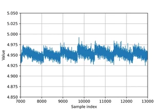 Image credit: [Me]
Maintaining stable DC voltages in modern electronic devices is a foundational challenge in embedded systems. Even slight fluctuations in the power supply can compromise performance, leading to data corruption, timing errors, or outright failure. These fluctuations, collectively known as voltage ripple, must be meticulously analyzed to ensure the robustness and reliability of a hardware design.
In this post, I’ll dive into a practical case study, analyzing the voltage ripple on a specific 5V rail within a complex, multi-source embedded system. By employing simple, readily available tools, namely a high-speed ADC and statistical processing, I’ll demonstrate how basic measurements can yield critical, non-destructive insights into power integrity.
This case study helped me to achieve an initial, non-oscilloscope evaluation of the power delivery network. At least until I have access to one.Specifically, I quantified key parameters such as:
- Peak and RMS voltage ripple: For precise power quality assessment.
- System stability: Determining if the ripple remains within tolerable operational bounds.
- Design effectiveness: Providing a fundamental evaluation of the power supply network’s overall robustness.
My analysis explored how different power sources, such as an USB adapter vs. a wireless receiver, introduce distinct and measurable ripple signatures, providing a tangible comparison for designing robust hardware.
Voltage ripple basics
Voltage ripple is defined as the periodic (or quasi-periodic) fluctuation superimposed on the DC rail. It arises from the designed power supply topology interacting with the parasitic characteristics of the passive components and the PCB itself.
To analyze it, we separate the waveform into its DC component (mean voltage) and ripple component (AC fluctuations).
For sampled waveform data $v[n]$ , the estimated DC value is:
$$V_{DC} = mean(v[n])$$Removing the DC component, the ripple is represented as:
$$V_{ripple}[n] = v[n] - V_{DC}$$The total voltage swing is:
$$V_{ripple, pp} = max(v[n]) - min(v[n])$$And the RMS value is calculated as:
$$V_{ripple,RMS} = \sqrt{ {\dfrac{1}{N}} {\sum_{n=0}^{N-1} (v[n] - V_{DC})^2} }$$Excess ripple is detrimental, because it leads to increased thermal stress and electromagnetic interference (EMI). If the instantaneous voltage drops below a device’s brownout threshold, a reset occurs. Large excursions can also disturb sensitive analog blocks, leading to measurable sampling errors and data corruption.
The allowable ripple varies widely depending on the component. While a general starting point for microcontrollers and microprocessors is the 1% rule of thumb to ensure clean logic thresholds, actual requirements differ. For example, some components specify ripple tolerances up to ±5%, while high-speed interfaces (like DDR5 RAM) require peak voltage ripple tolerances as low as 0.2%.
When measuring ripple, knowing which metric to focus on is critical. RMS values give an indication of the total power dissipated as heat. Peak-to-peak values determine the instantaneous rail voltage variation and is crucial for assesing the risk of brownout resets or analog circuit degradation.
The specific shape of the ripple signal is key to troubleshooting. When the output capacitor’s ESR is significant, the ripple voltage contains a component that mirrors the ripple current waveform, often quasi‑rectangular because the regulator switches a constant current into the inductor. When ESR is low, the voltage ripple is dominated by the capacitor’s charging and discharging, giving a near‑triangular (or sawtooth) shape. With very low‑ESR ceramics, the ESR‑induced rectangular component becomes small, so the voltage ripple continues being primarily the capacitive charging and discharging of the output capacitor, yielding a fairly sinusoidal shape.
Regardless of whether the ripple has a particular shape or not, sometimes observing the visual waveform is not enough. If you can, use an oscilloscope to perform a detailed analysis. A deeper dive allows you to identify subtle harmonic components that can significantly impact the stability and function of your hardware design.
Methodology
While the preceding section provided theory for analyzing ripple, this section anchors that knowledge to a practical, real-world hardware design. The system under test is a complex embedded design, which presents multiple potential ripple hazards, including inherent ripple from low-dropout regulators (LDOs), transient switching noise from the power switchover circuitry, and the interaction between two distinct power sources: a LiPo battery and inductive wireless power.
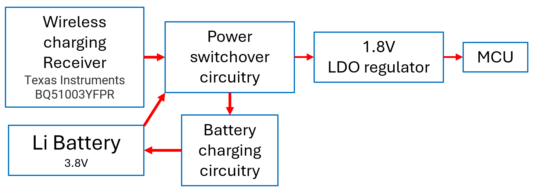
Figure 1. The real-world design for which the voltage ripple will be analyzed.
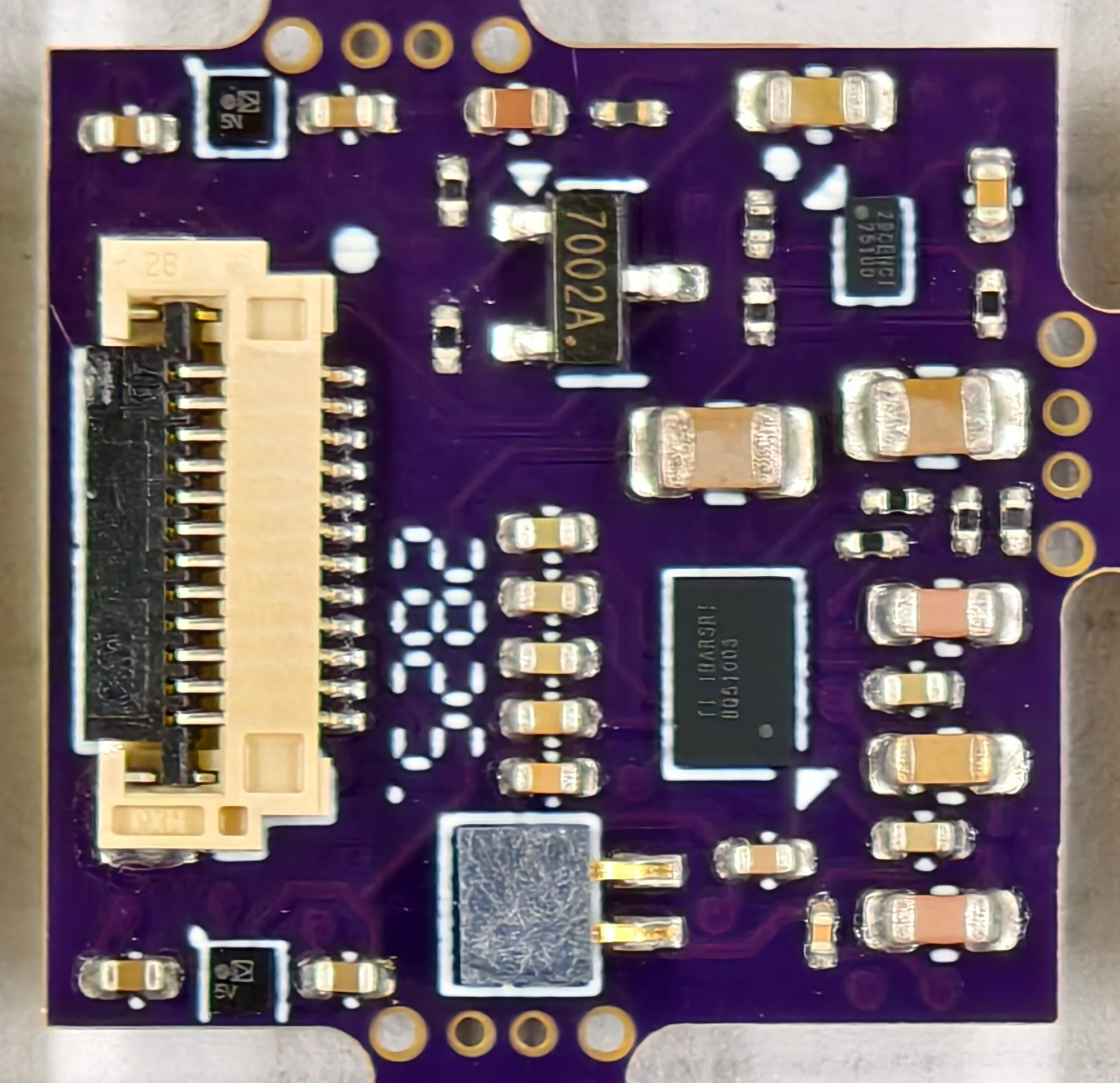
Figure 2. Part of the PCB design that generates a 5V rail, as the power switchover circuit output.
For the presented design, I wanted to examine the 5V voltage rail that a LDO regulator receives, operating in ordinary conditions and other sudden changes of load current, for a short time interval. This device’s hardware system has two available power sources: a 3.8V LiPo battery, and a wireless charging receiver circuit employing an inductive coil. Their results will be compared against a 5V rail from a USB adapter.
A dedicated power switchover circuitry manages power delivery. It prioritizes the use of wireless power when available; otherwise, it switches to battery power. The hardware also includes dedicated battery charging circuitry to protect the wireless receiver IC from thermal runaway. The power switchover circuitry transmits power to multiple low-drop voltage regulators, including a 1.8V voltage rail for a microcontroller. The objetive is to ensure this rail remains within the required tolerance regardless of which source is active, by analyzing how signals and frequency components behave under 500 kHz.
To conduct this analysis, I designed a custom data acquisition pipeline. I used the XADC module from an AMD Zynq-7000 SoC, which has a synchronized and verified 1 MSPS sampling rate. To handle the large volumes of captured data, an FPGA architecture was elaborated, incorporating high-speed DMA (Direct Memory Access) for safe and efficient storage of all measurements.
I took $10^7$ continuous samples per capture. That is equivalent to 10 seconds. This duration was sufficient to capture multiple operational cycles and establish an initial statistical baseline to characterize noise and repeatable ripple patterns.
The signals to measure go to an LM318 op-amp with some voltage dividers, configured as a buffer with high input impedance. The LM318’s buffer bandwith (1 MHz) ensured minimal distortion, but its finite input impedance (1 MΩ) required careful grounding to avoid common-mode noise.
It is important to note that the data acquisition was configured to monitor the voltage rails under load conditions, specifically excluding the detailed analysis of the power switchover circuit’s internal switching behavior. The scope of this post is strictly limited to analyzing the resulting voltage rails that experience both static and transient current changes.
Results
Comparison of 5V sources
The first phase of my analysis focused on the main 5V rail, comparing two vastly different external power sources: a commercial USB adapter and a dedicated inductive wireless receiver. Analyzing these rails allowed me to benchmark the ripple characteristics introduced by the power sources.
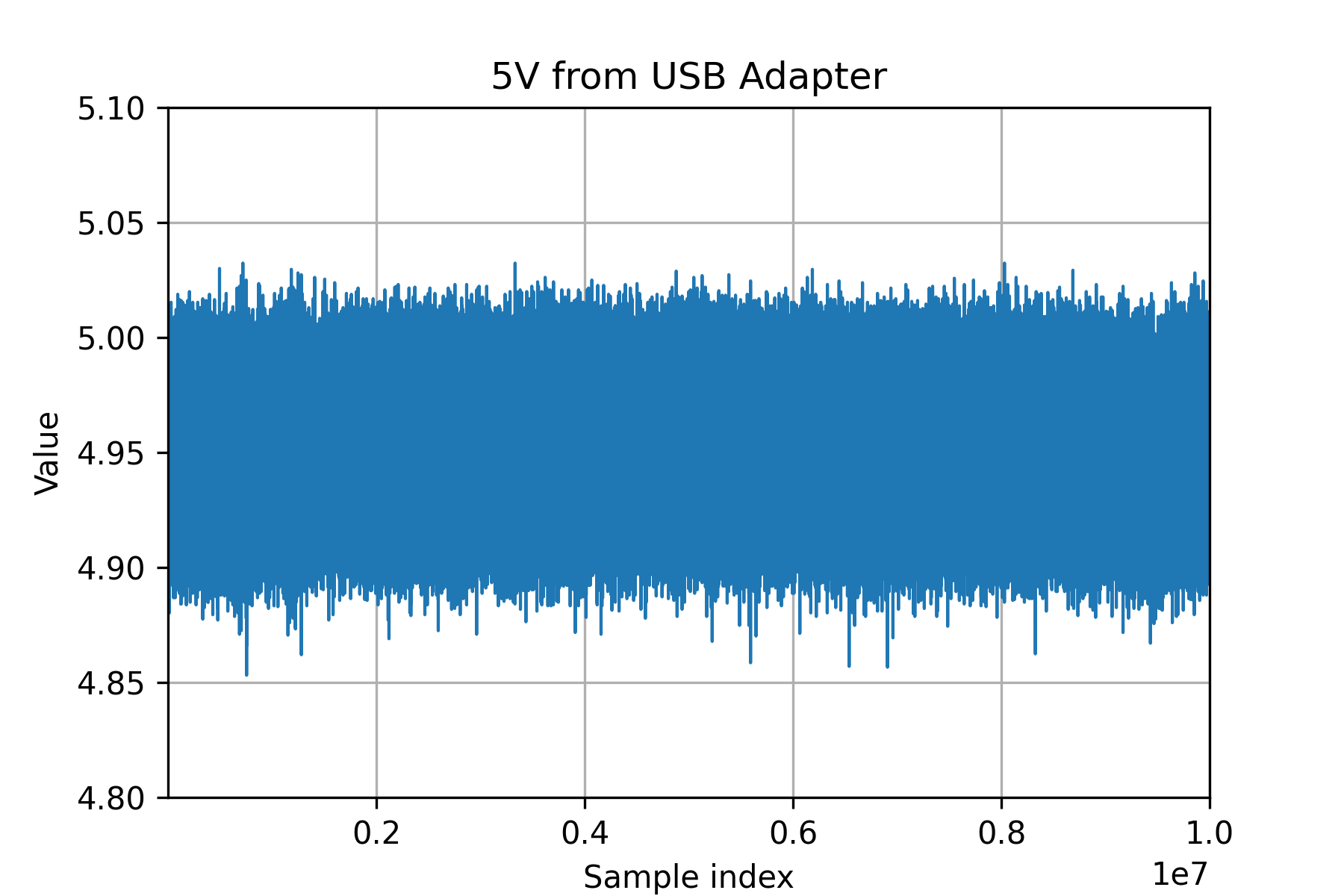
Figure 3. Overall waveform capture of a 5V rail coming from an USB output from an adapter. Visually, this rail has an average 4.95V, and fluctuates between 4.85V and 5.05V.
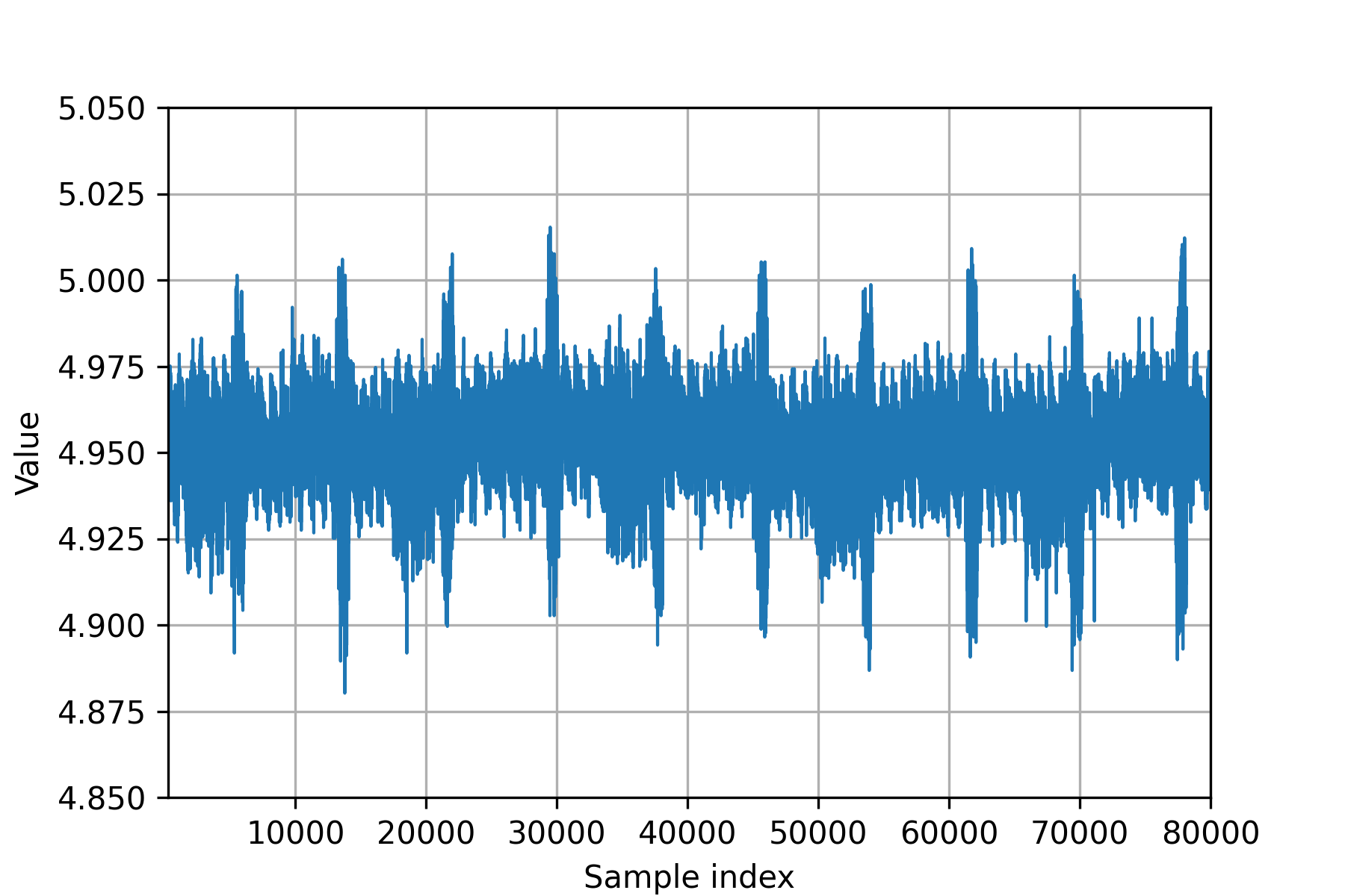
Figure 4. First 80000 samples. There is a quasi-periodic signal pattern.
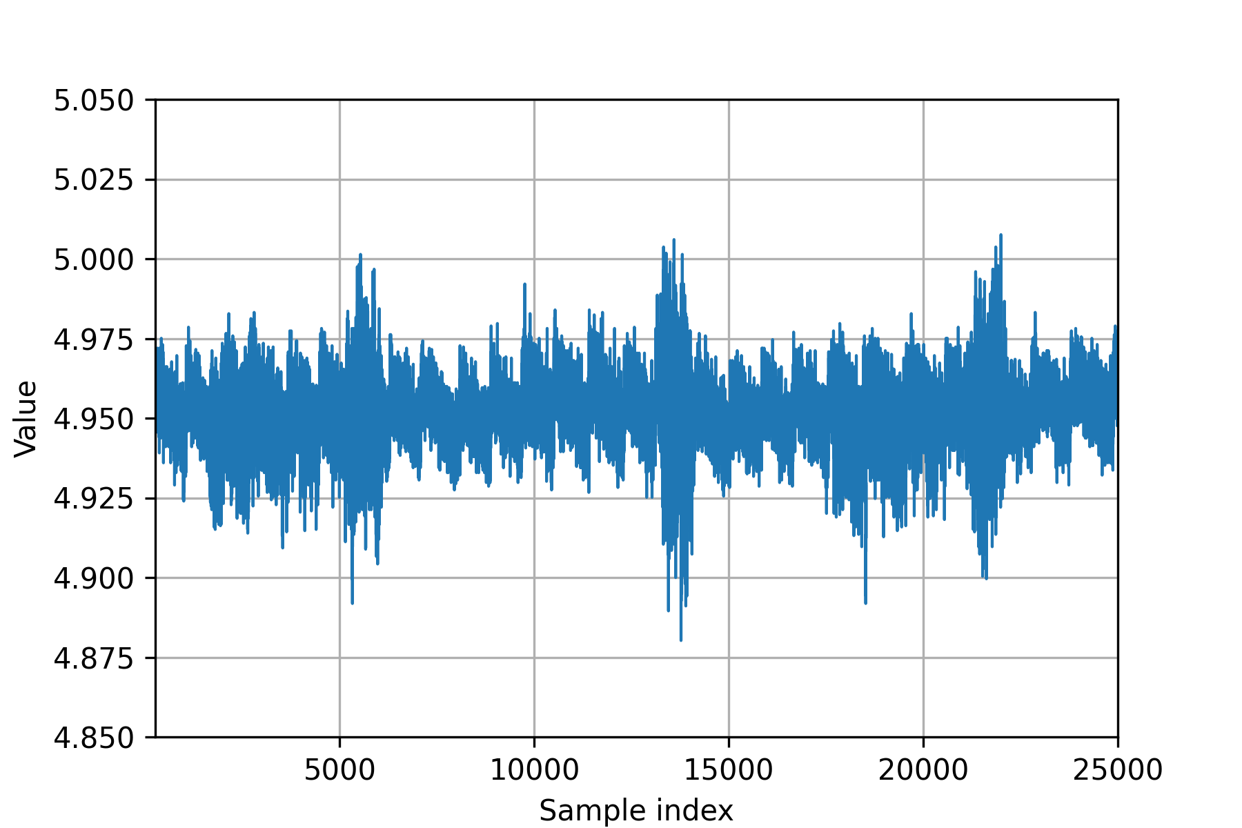
Figure 5. Amplifying the quasi-periodic signal pattern.
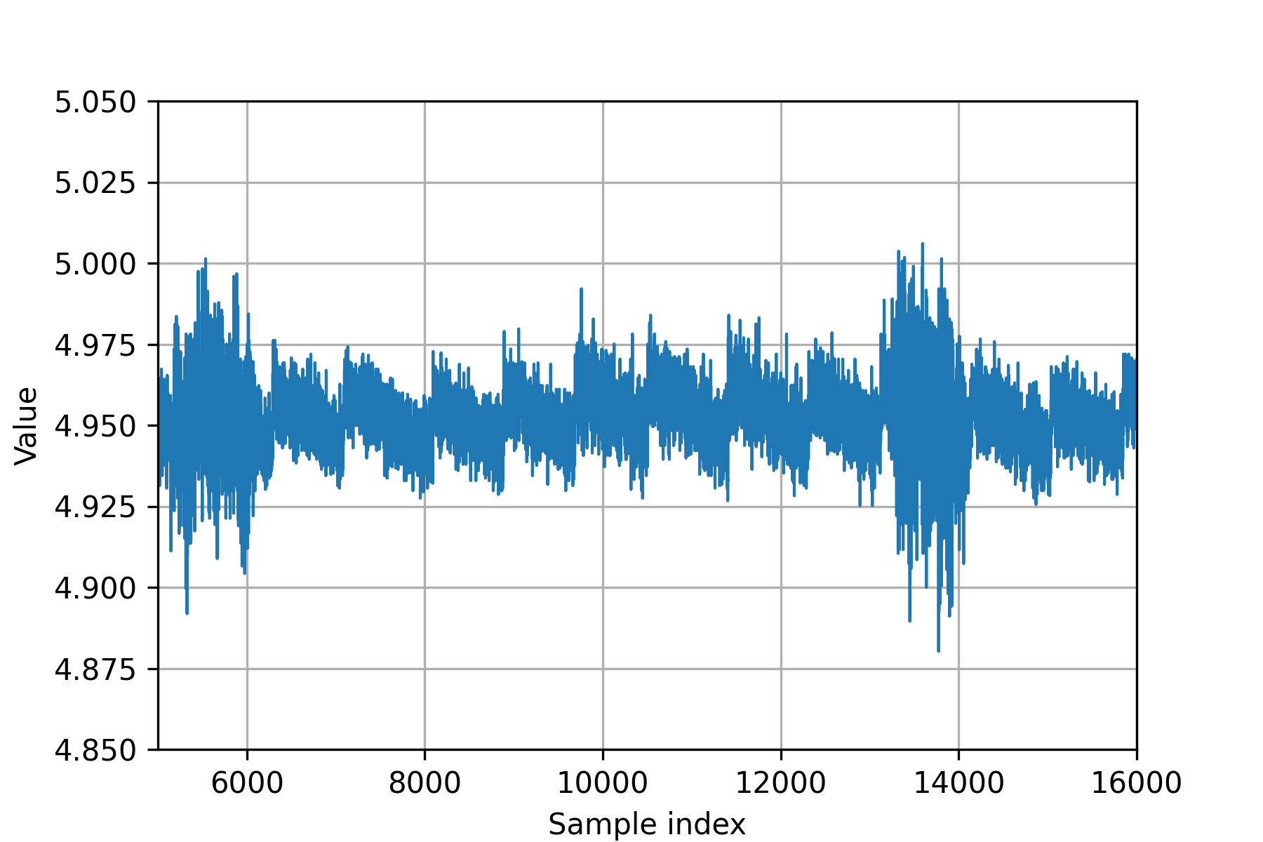
Figure 6. The quasi-periodic signal pattern has a capacitor discharge behavior, with some pulse bursts that also seem periodic.
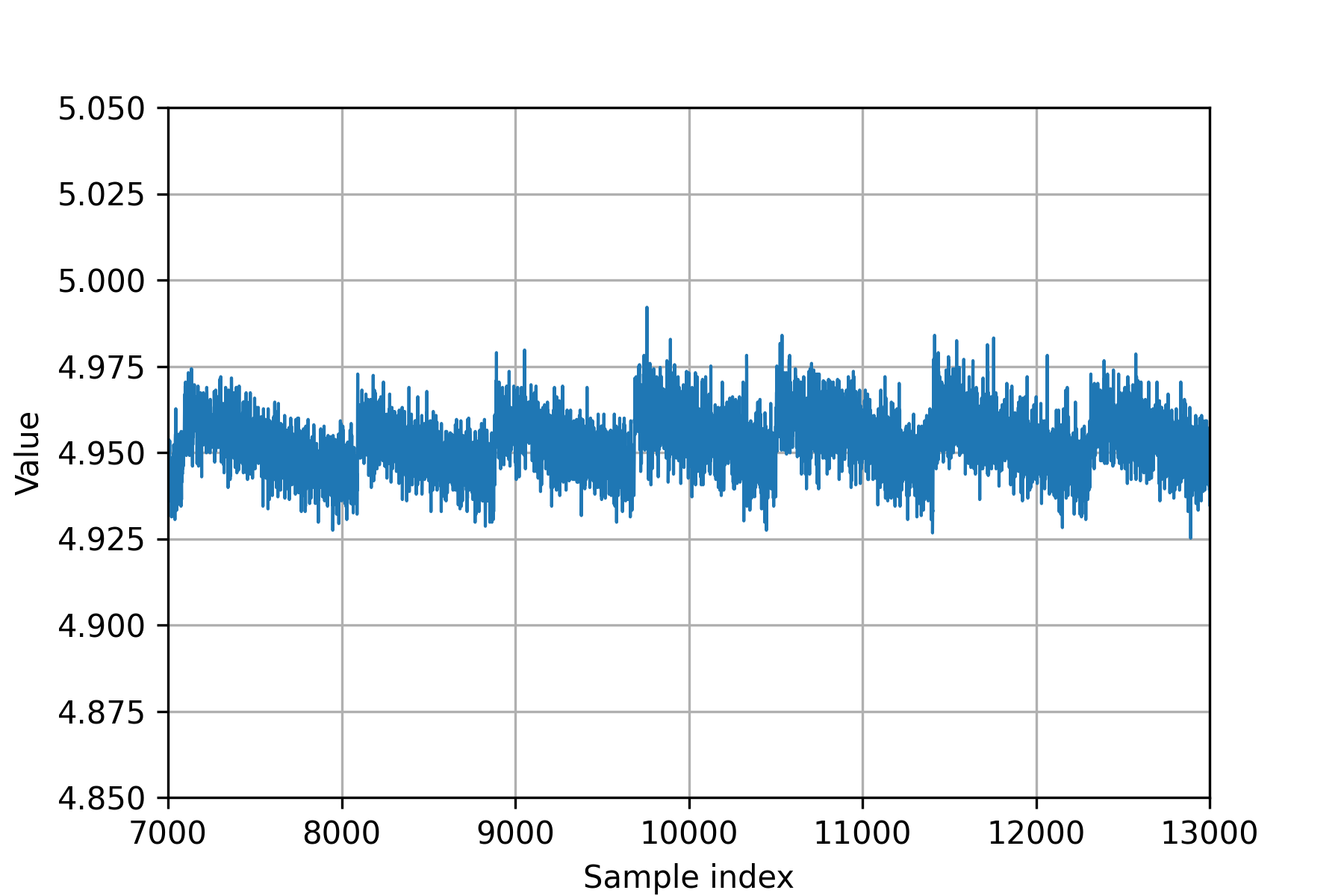
Figure 7. Detail of the capacitor discharge periodic signal. Each discharge cycle lasts about 0.8 ms.
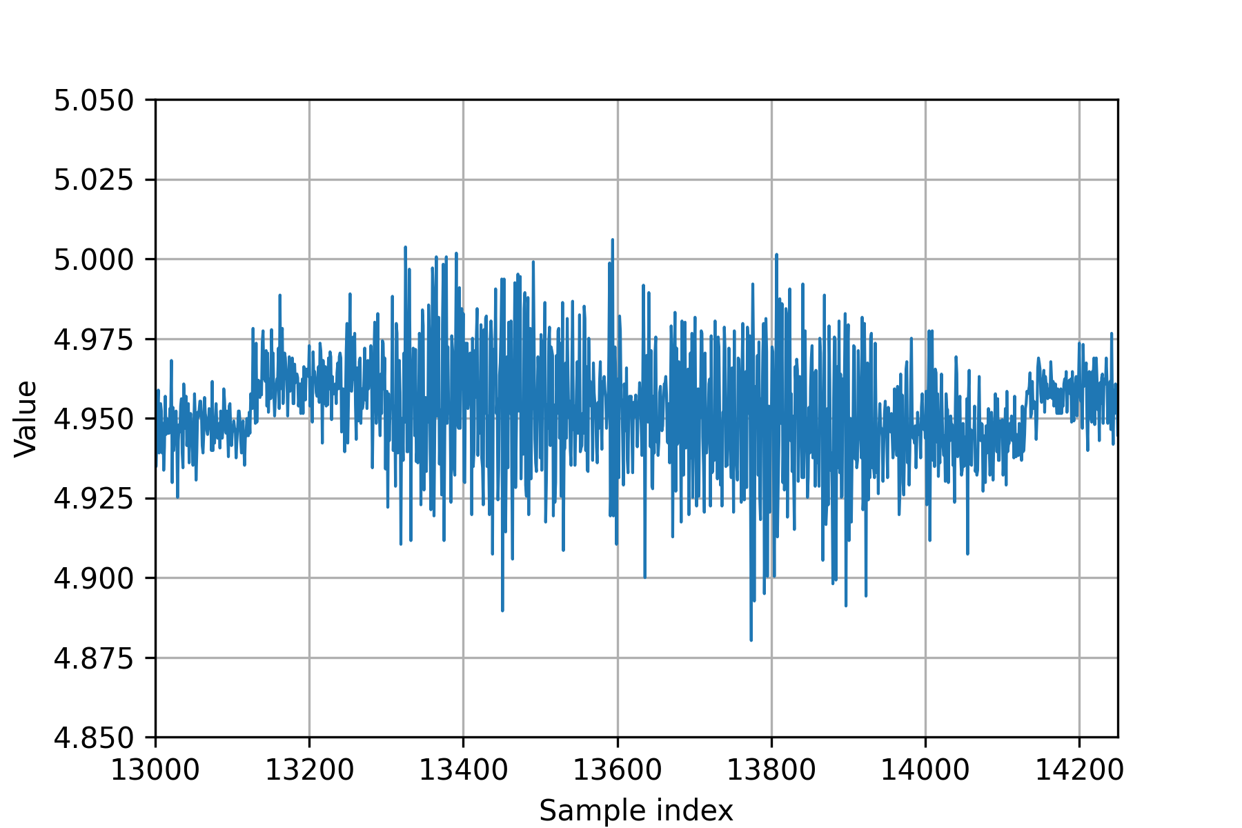
Figure 8. Detail of the pulse bursts. The 1MSPS sampling rate doesn’t allow to see faster signals.
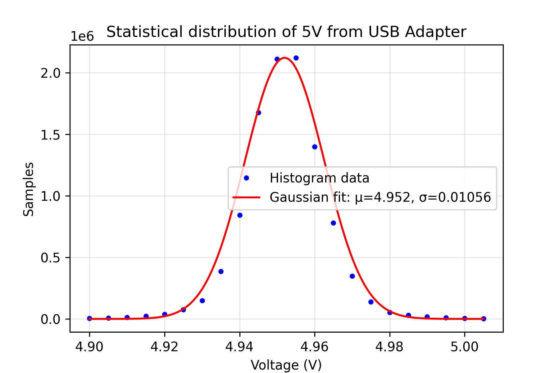
Figure 9. Statistical distribution of 5V measurements. The 5V rail coming from the USB adapter fluctuates between 4.92V and 4.98V.
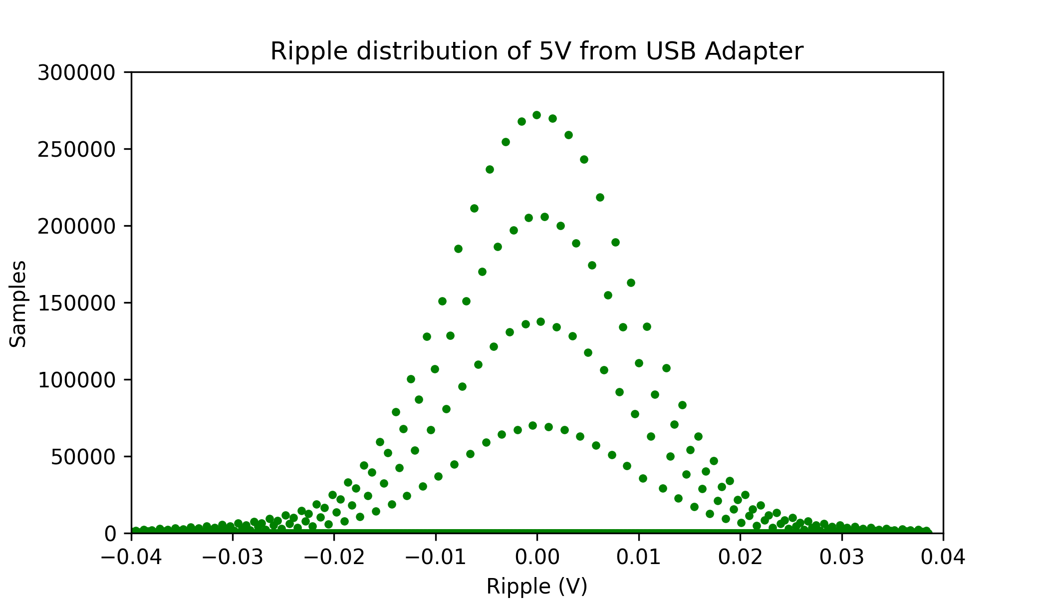
Figure 10. The ripple distribution of 5V measurements reveals that its waveform components are periodic.
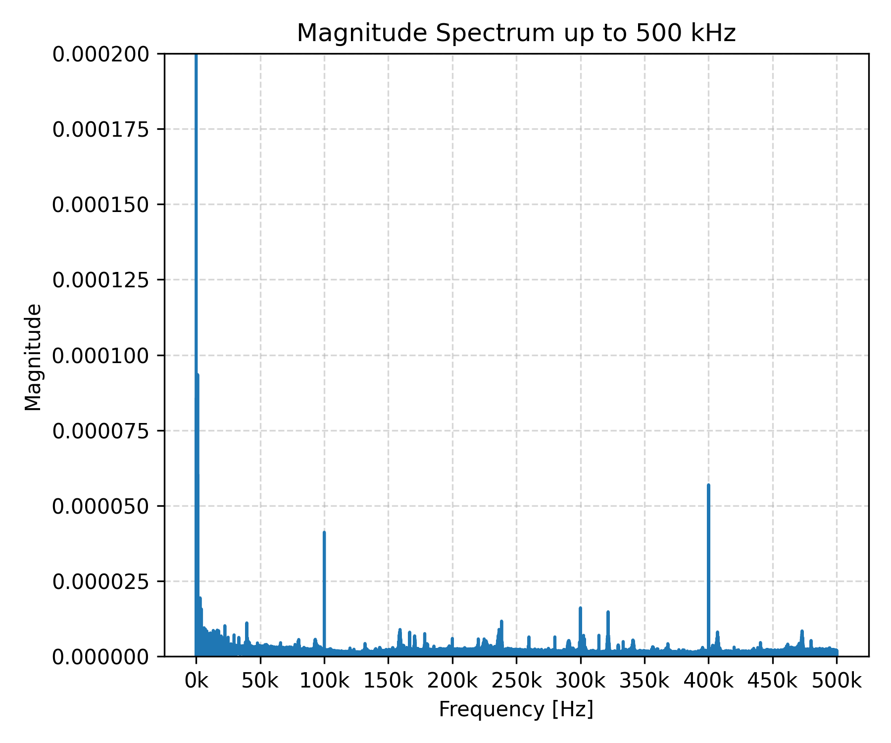
Figure 11. Magnitude spectrum of 5V coming from the USB adapter. There are two frequency components that stand out at 100 KHz and 400 kHz.
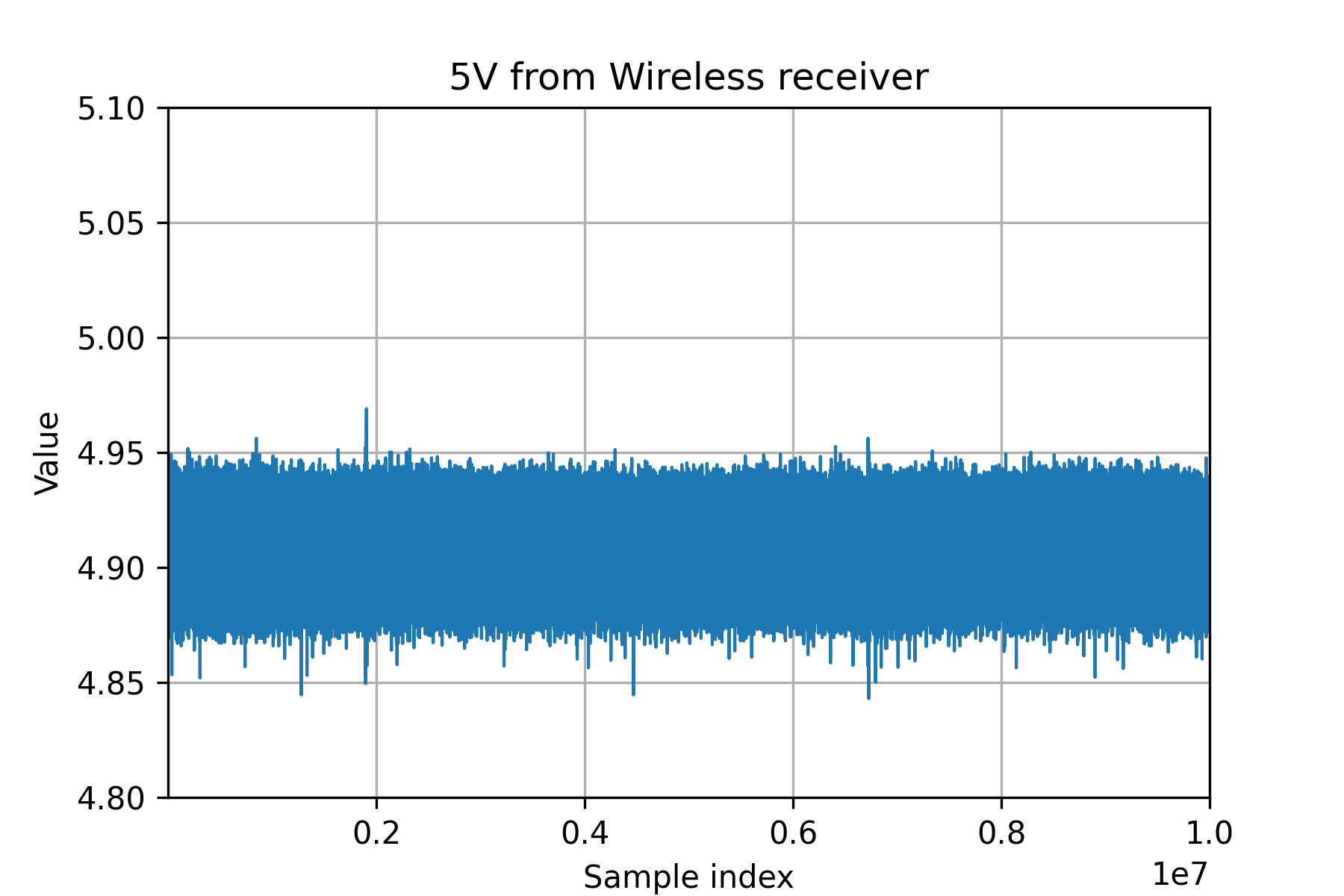
Figure 12. Overall waveform capture of a 5V rail coming from the wireless receiver output. Visually, this rail has an average 4.90V, and fluctuates between 4.85V and 4.95V.
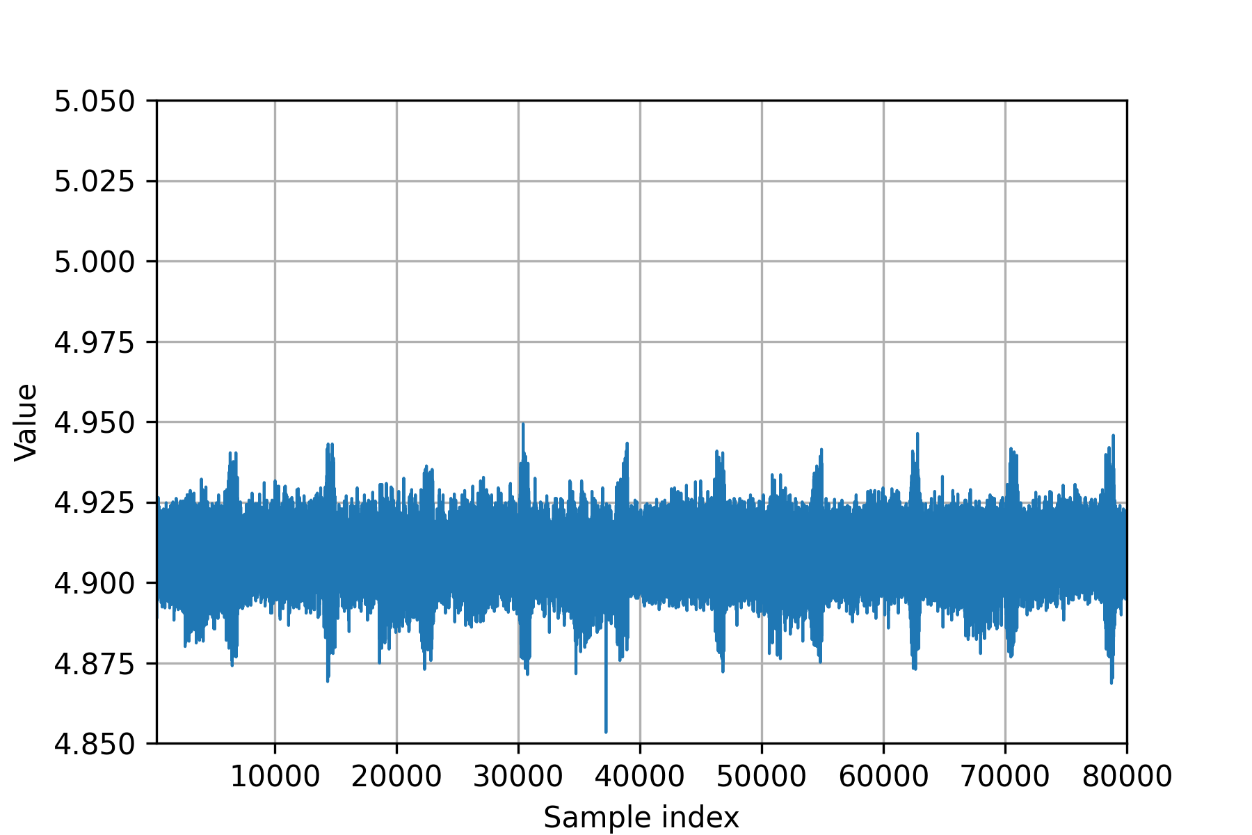
Figure 13. First 80000 samples. There is a quasi-periodic signal pattern.
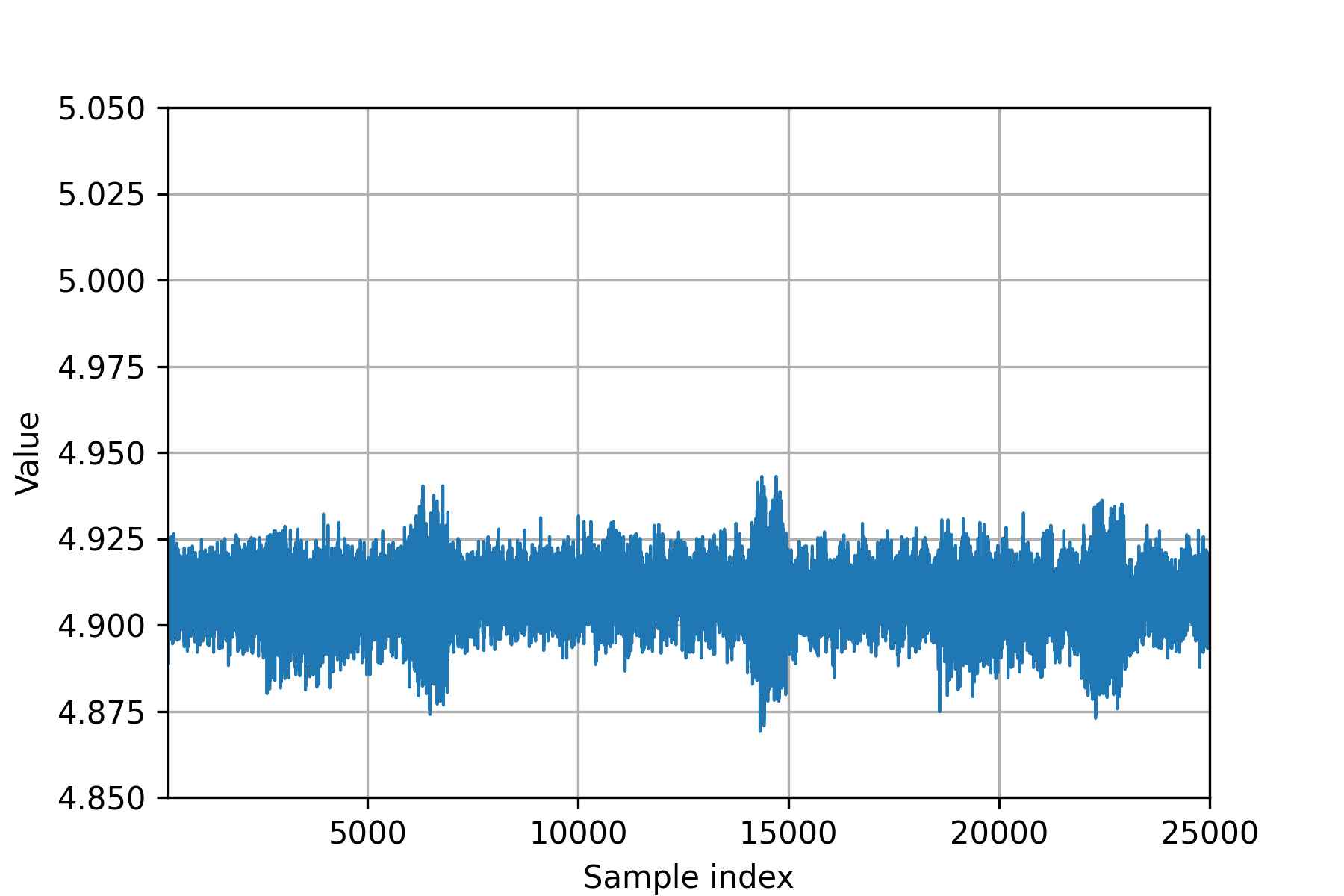
Figure 14. Amplifying the quasi-periodic signal pattern.
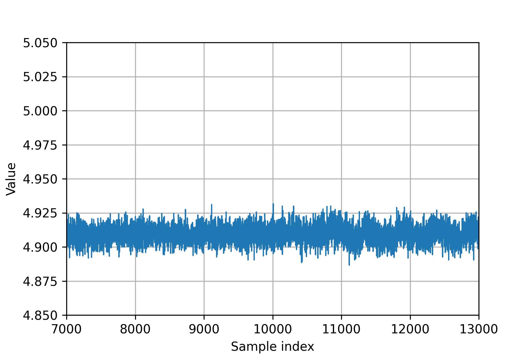
Figure 15. Detail of the spaces between the pulse bursts. The ripple is smoother because of low-ESR ceramic capacitors.
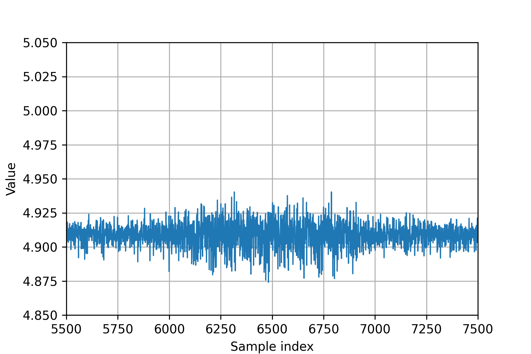
Figure 16. Detail of the pulse bursts. The 1 MSPS sampling rate doesn’t allow to see faster signals.
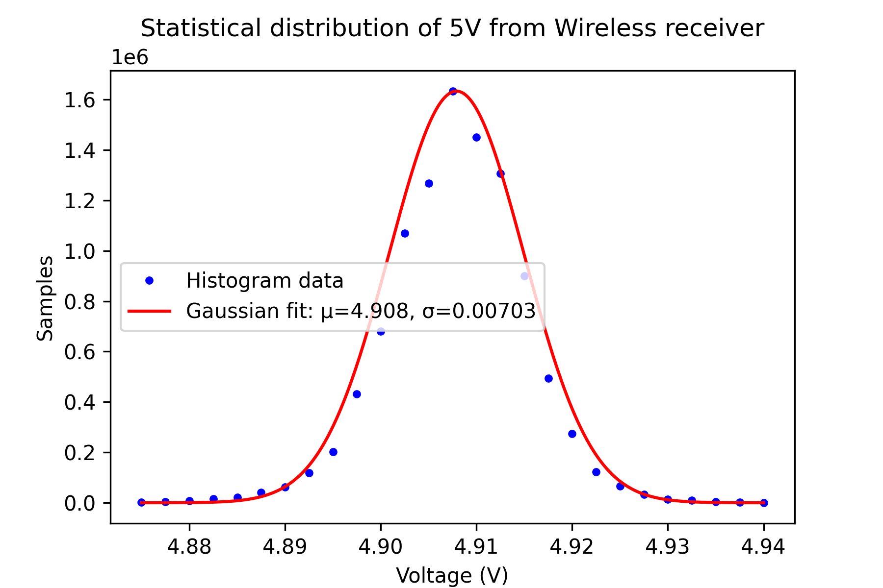
Figure 17. Statistical distribution of 5V measurements. The 5V rail coming from the USB adapter fluctuates between 4.89V and 4.93V.
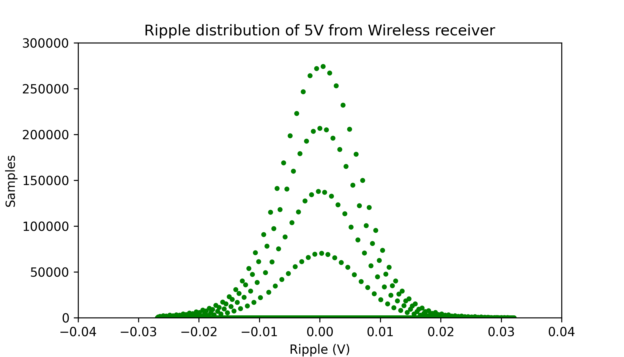
Figure 18. The ripple distribution of 5V measurements also reveals that its waveform components are periodic.
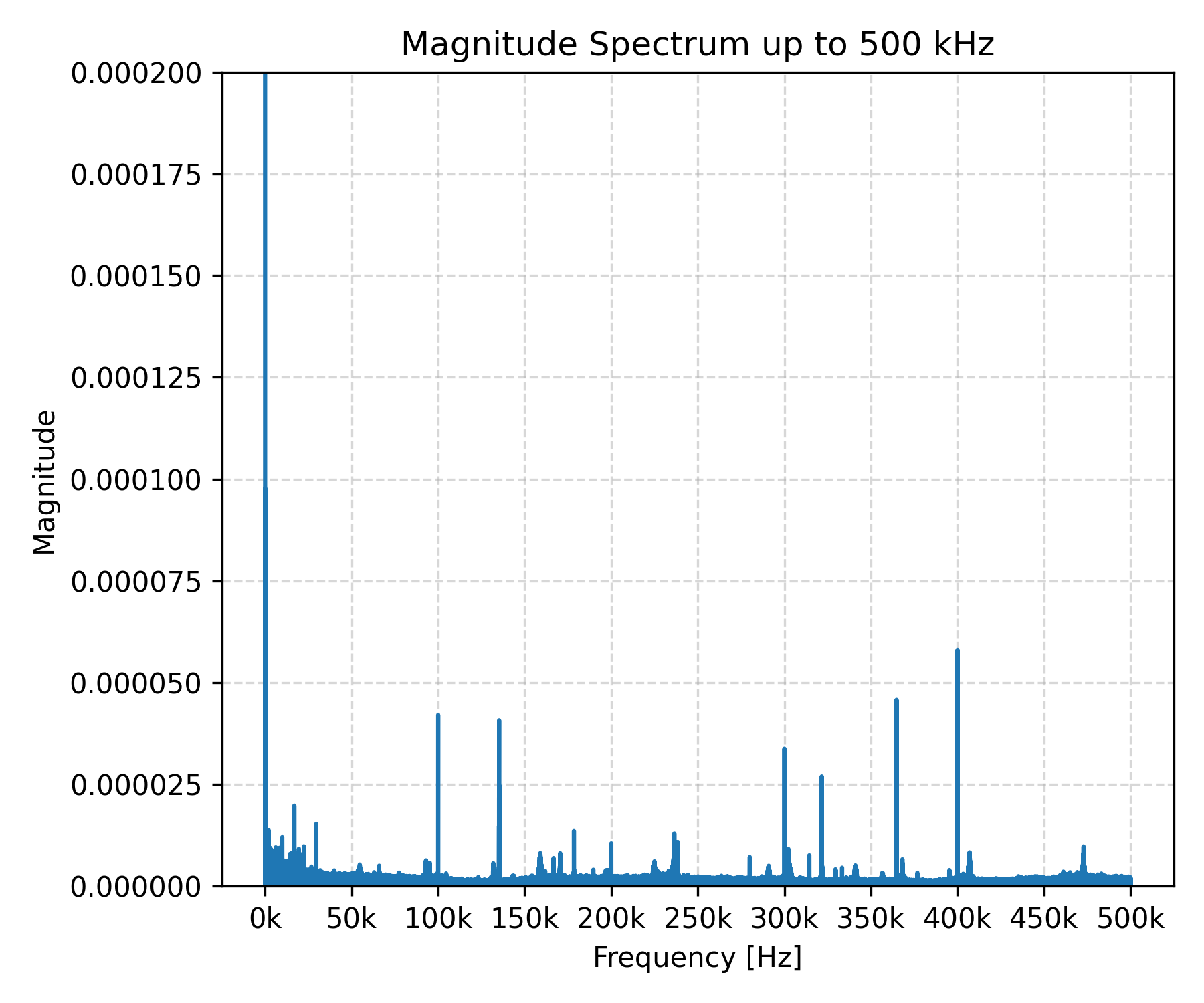
Figure 19. Magnitude spectrum of 5V coming from the wireless receiver. Compared to the 5V coming from the USB adapter, this rail has some additional spectrum components.
The measurements calculated are:
| Measurement | 5V from USB adapter | 5V from wireless receiver |
|---|---|---|
| Mean voltage (V) | 4.955 | 4.909 |
| Max voltage (V) | 5.032 | 4.969 |
| Min voltage (V) | 4.853 | 4.843 |
| Ripple p-p (V) | 0.179 | 0.126 |
| Ripple RMS (V) | 0.011 | 0.007 |
| Ripple percentage, p-p | 3.618 % | 2.567 % |
| Ripple percentage, RMS | 0.213 % | 0.143 % |
Table 1. Calculated differences between 5V rails from the USB adapter and the wireless receiver.
The initial waveform capture (Figure 4) of the 5V from the USB adapter revealed a clear, fluctuating signal. Visually, it fluctuated between 4.85V and 5.05V. The following figures showed a pronounced, quasi-periodic ripple pattern characterized by sharp, recurring pulse bursts. This suggests the ripple is heavily influenced by the load’s instantaneous current draw, likely due to internal regulation and power delivery cycles.
In contrast, the 5V from the wireless receiver (Figure 14) revealed a significantly smoother waveform. The fluctuation was contained between 4.85V and 4.95V. The following figures show that the signal is markedly smoother than the USB source. The spaces between the pulse bursts are notably cleaner, suggesting that the power transfer mechanism or the integrated low-ESR ceramic capacitors are performing better at filtering part of the ripple.
While both sources exceed the general microcontroller “1% rule of thumb”, the resulting ripple remains within a permissible 5% peak-to-peak window for the specific application the PCB is designed for. However, this analysis highlights significant differences in power quality that directly impact hardware reliability.
A critical consideration is the source quality. If the device were charged or powered by a low-quality or poorly regulated USB adapter, the ripple could easily spike far beyond the measured 3.6% p-p, potentially approaching the 5% threshold. Such excessive fluctuations could cause voltage-sensitive analog blocks to suffer degradation or even trigger brownout resets, compromising the system’s core functionality.
Comparison of 1.8V sources
The second phase of my analysis involved examining the 1.8V voltage rail, the core operating voltage for the microcontroller. This rail is generated by an LDO (Low Dropout Regulator) that receives its input power from the main 5V rail. Therefore, the ripple observed here is not only the source ripple itself, but the residual ripple, the component of fluctuation that the LDO was unable to entirely filter out.
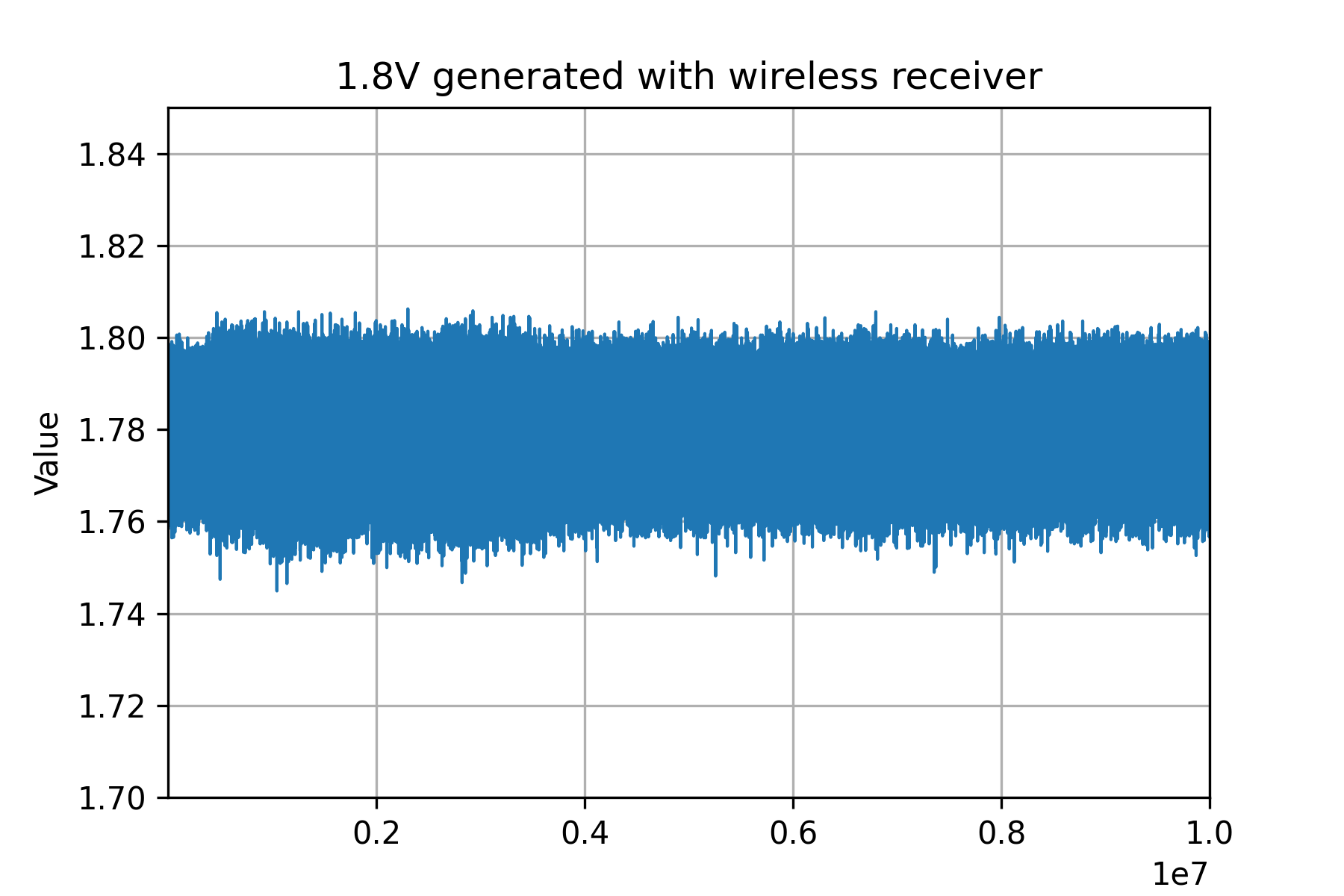
Figure 20. Overall waveform capture of a 1.8V rail generated with the wireless receiver. Visually, this rail has an average 1.78V, and fluctuates between 1.75 and 1.81V.
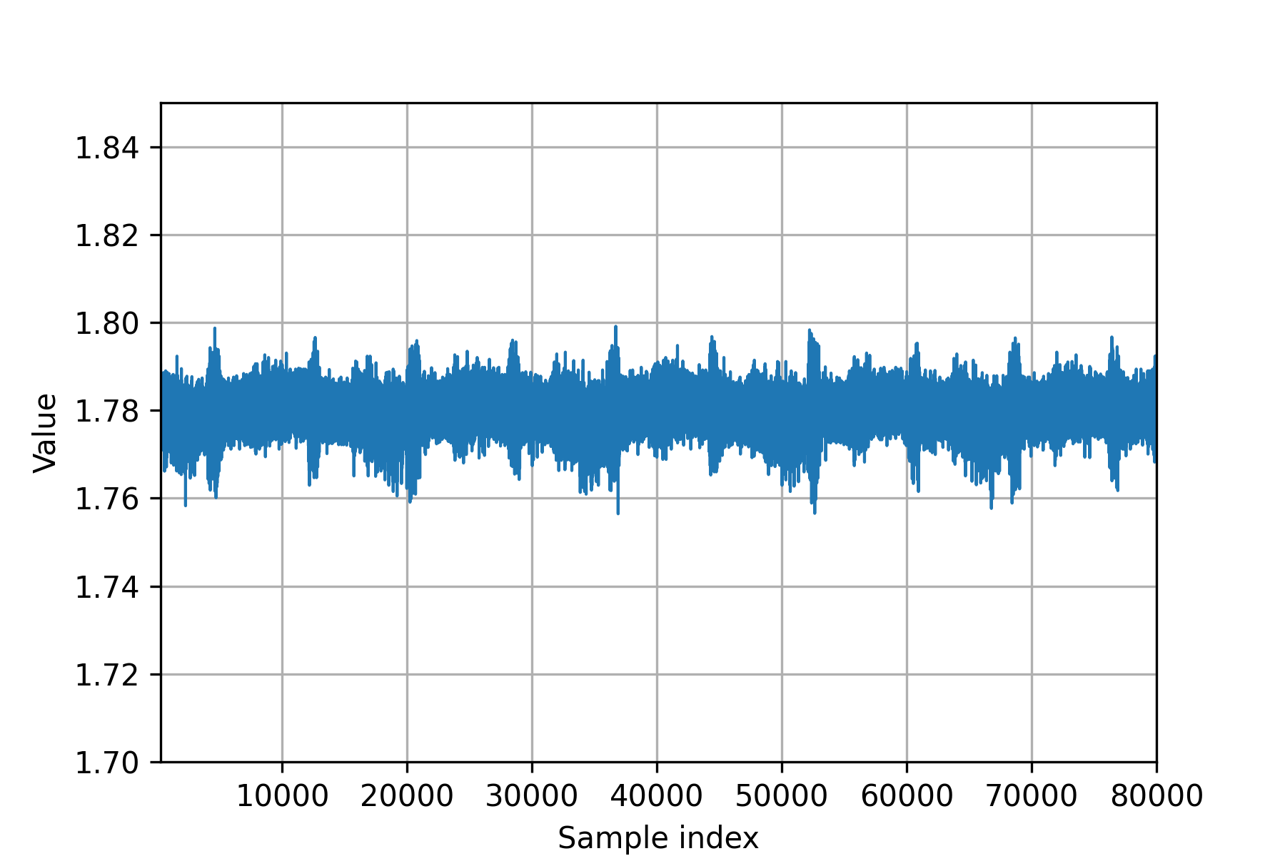
Figure 21. First 80000 samples. The quasi-periodic signal pattern appears again.
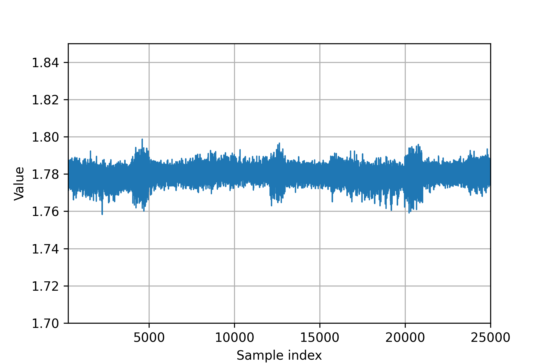
Figure 22. Detail of the spaces between the pulse bursts. The ripple is smoother because of low-ESR ceramic capacitors. However, there might be faster signals that aren’t captured.
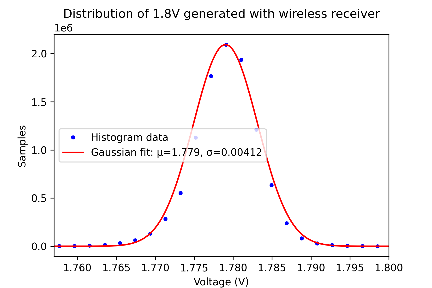
Figure 23. Statistical distribution of 1.8V measurements for the rail generated with the wireless receiver.
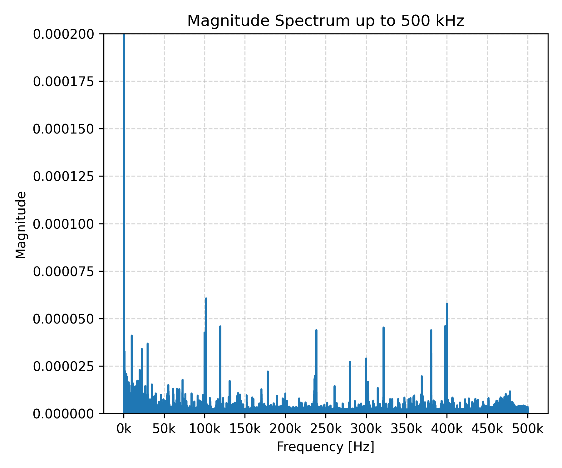
Figure 24. Magnitude spectrum of 1.8V generated with the wireless receiver. Compared to the 5V rails, more spectral components appear.
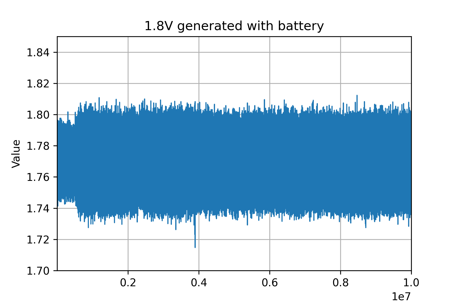
Figure 25. Overall waveform capture of a 1.8V rail generated with the LiPo battery. Visually, this rail has an average 1.78V, and fluctuates between 1.74 and 1.82V.
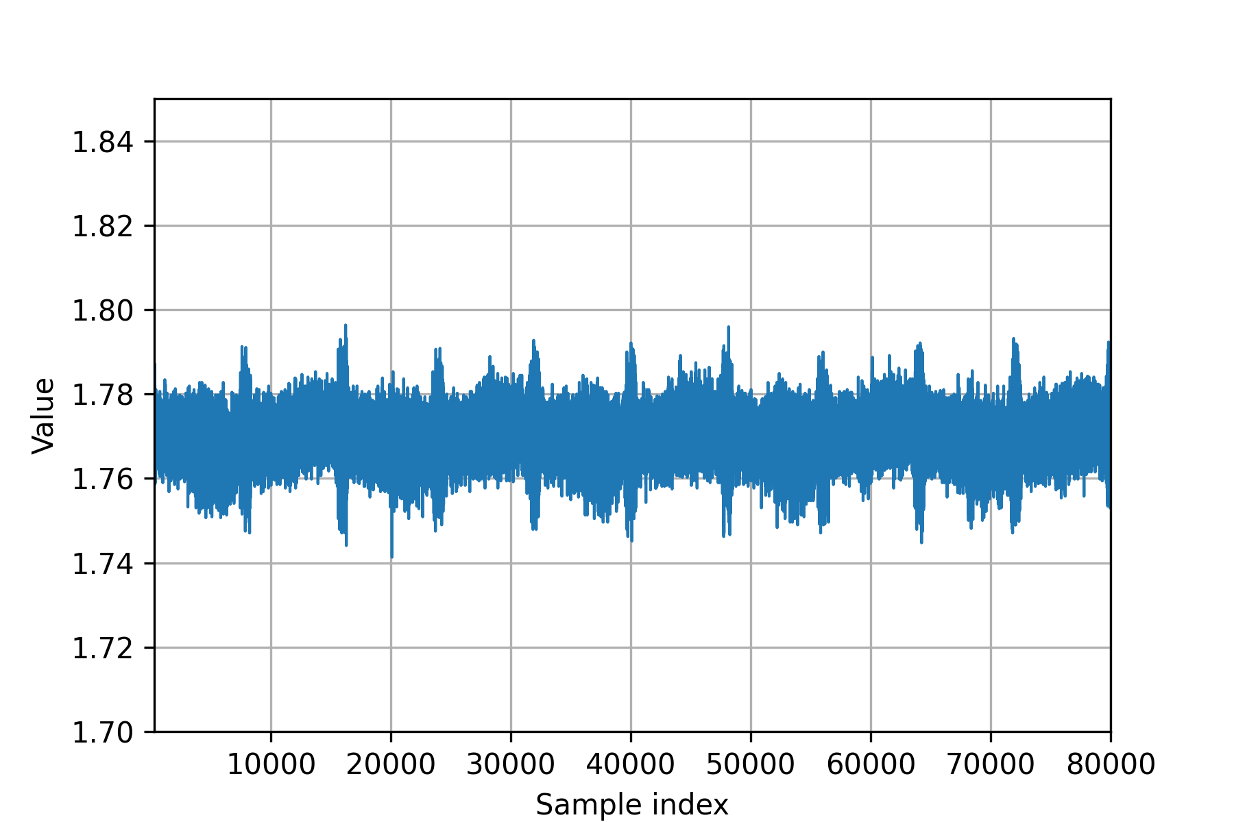
Figure 26. First 80000 samples. The quasi-periodic signal pattern one more time.
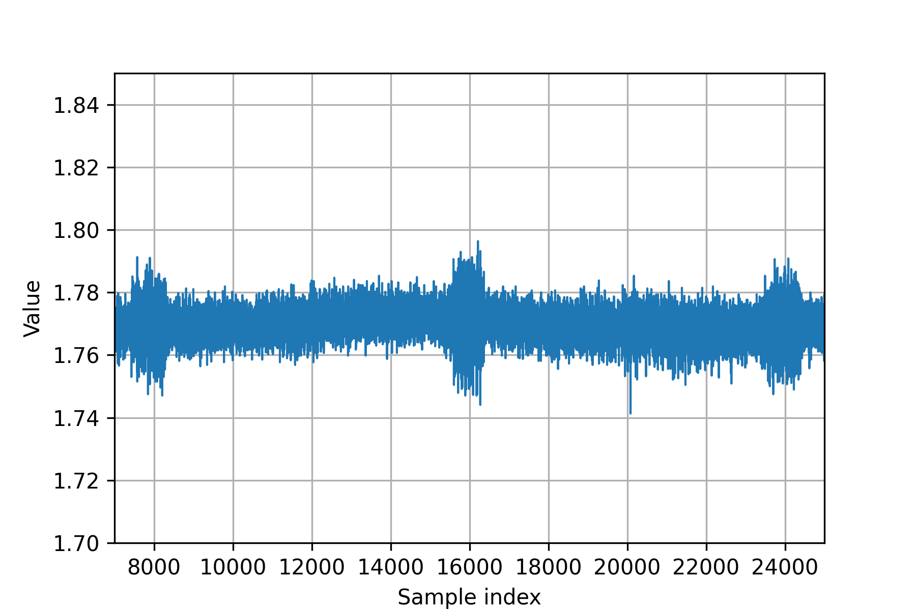
Figure 27. Detail of the spaces between the pulse bursts. The ripple is smoother because of low-ESR ceramic capacitors. Again, there are faster signals that aren’t captured.
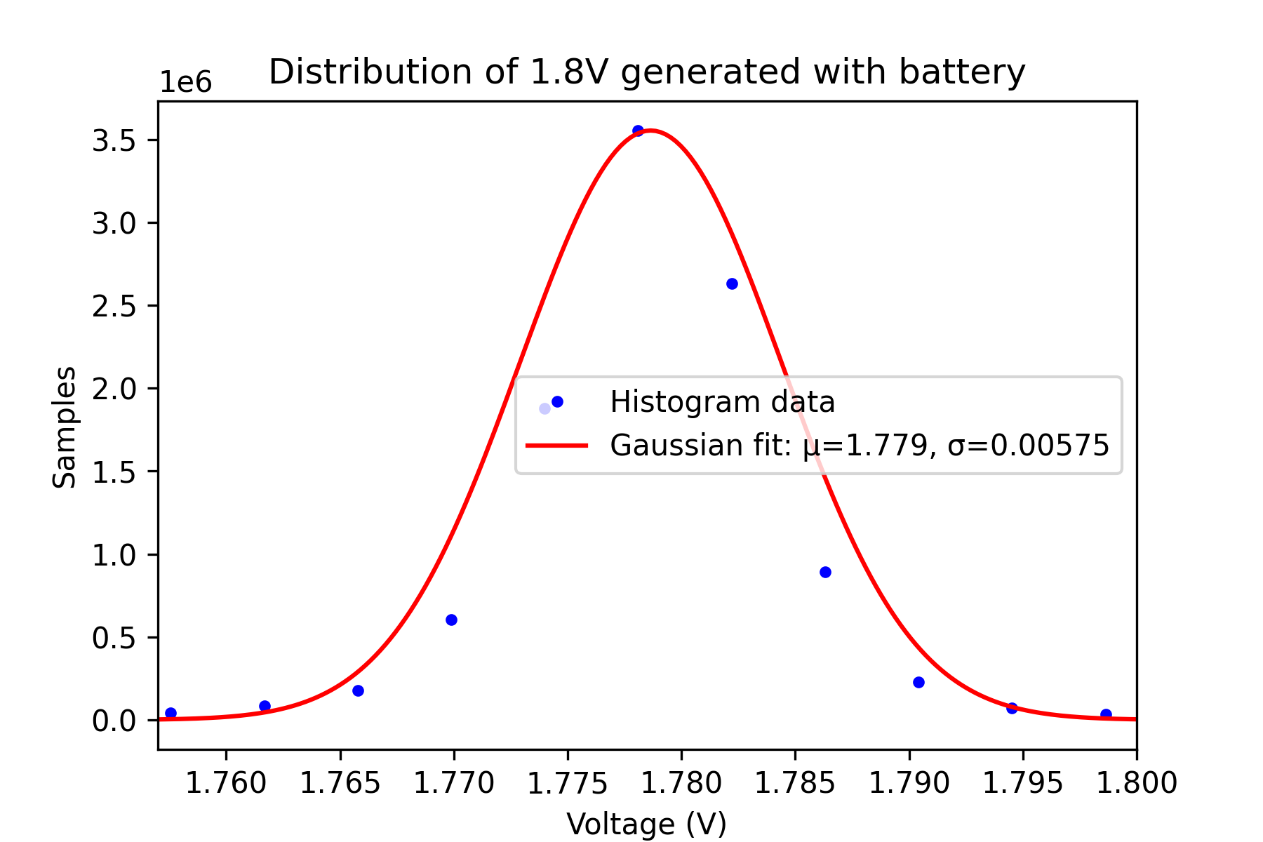
Figure 28. Statistical distribution of 1.8V measurements, for the rail generated with the battery.
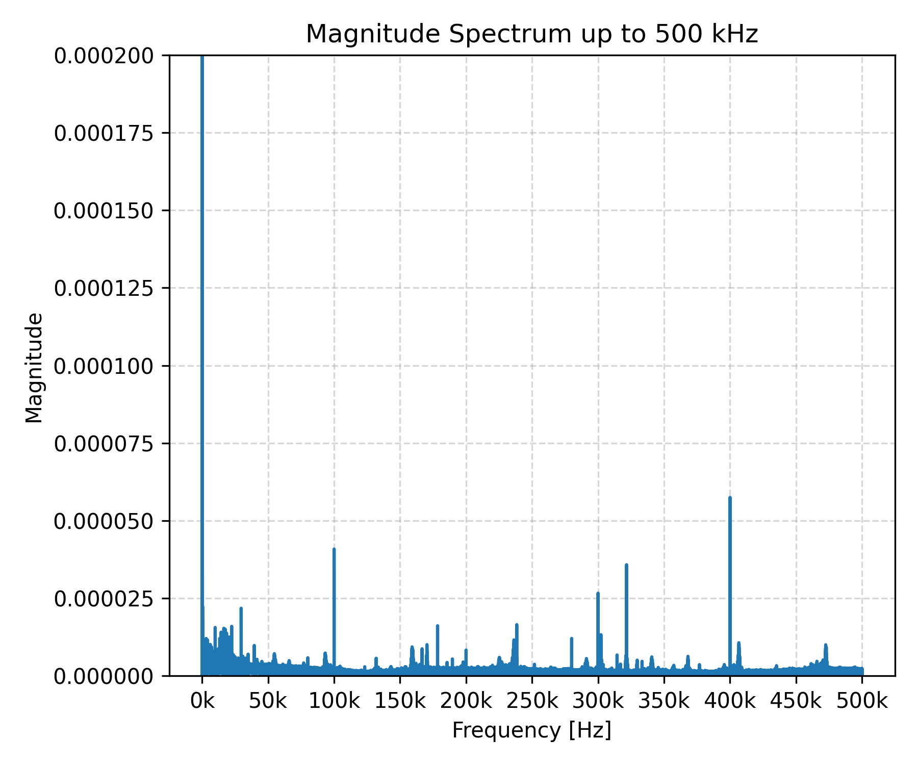
Figure 29. Magnitude spectrum of 1.8V generated with the battery. Compared to the 5V and 1.8V rails that use the wireless receiver, battery usage adds less harmonic components.
The overall waveform captures (Figures 21 and 26) confirm that ripple exists across both sources. The LDO regulator is performing its job by regulating the DC mean voltage (maintaining the rail close to 1.8V), but the dynamic load changes and input ripple propagate into measurable fluctuations.
Comparing the wireless (Figure 22) and battery (Figure 27) sources visually reveals similar transient behaviours, characterized by (again) pronounced periodic pulse bursts. This consistency suggests that the load profile is the primary driver of the transient switching noise, regardless of the primary voltage source.
| Measurement | 5V from USB adapter | 5V from wireless receiver | 1.8V from wireless receiver | 1.8V from LiPo battery |
|---|---|---|---|---|
| Mean voltage (V) | 4.955 | 4.909 | 1.780 | 1.770 |
| Max voltage (V) | 5.032 | 4.969 | 1.806 | 1.812 |
| Min voltage (V) | 4.853 | 4.843 | 1.745 | 1.715 |
| Ripple p-p (V) | 0.179 | 0.126 | 0.061 | 0.098 |
| Ripple RMS (V) | 0.011 | 0.007 | 0.004 | 0.006 |
| Ripple percentage, p-p | 3.618 % | 2.567 % | 3.445% | 5.513 % |
| Ripple percentage, RMS | 0.213 % | 0.143 % | 0.230 % | 0.318 % |
Table 2. Calculated differences between the rails.
The quantitative results in Table 2 offer a clear comparison of power quality dynamics within the system. The primary takeaway is that while the Low Dropout Regulator (LDO) successfully performs its core duty, maintaining the mean DC voltage at the critical 1.8V, but it doesn’t act as a perfect filter. The measurable, non-zero ripple at the output indicates that external fluctuations and internal system transients are propagating into the sensitive microcontroller rail.
The initial comparison highlights that the ripple is highly sensitive to the input power source. The wireless source yielded a demonstrably cleaner 5V input, resulting in the lowest residual ripple (0.004V RMS) at the 1.8V output. This confirms that the quality of the upstream power delivery network (including the source and its immediate decoupling capacitors) are important to the overall system power integrity. Conversely, the combination of the battery source and load profile resulted in the highest measured ripple (0.006V RMS).
The LDO’s effectiveness is finite. It is designed to compensate for a specific, constrained range of voltage variations, but it cannot perfectly eliminate every high-frequency, transient noise component. The persistent periodic pulse bursts observed, even after passing through the regulator, confirm that the limiting factor is not the regulator itself, but the rate at which the load demands current (the dynamic load profile). This pattern strongly suggests that the ripple is predominantly generated by the load’s interaction with the system’s power switchover circuitry.
Given that the root cause of the residual ripple is the dynamic current demand of the load, achieving stricter voltage ripple requirements needs a redesign focused on mitigating transients. The following techniques could be implemented in future iterations:
- Optimized Decoupling Capacitance: Adding larger, strategically placed bypass and decoupling capacitors, particularly near the LDO input, helps absorb high-frequency transients.
- Layout Optimization (Minimizing ESL/ESR): Optimizing the PCB layout to minimize the parasitic inductance and resistance of power traces, thereby reducing the ripple magnitude.
- Low-Pass Filtering: Integrating an active or passive low-pass filter on the input power rail can effectively attenuate known harmonic components, significantly smoothing the signal.
The bottom line
This analysis demonstrates that basic high-speed ADCs and statistical analysis, without the need for a time-consuming oscilloscope setup, can reliably diagnose early critical power integrity hazards.
A robust power supply design must systematically address these domains of potential failure: input stages, PCB layout and load transient profiles. By managing them, we can transform the power delivery network from a potential weak point into a predictable, engineered strength.

I’m interested in:
• Firmware and embedded software development
• Instrumentation and sensor systems
• PCB design tailored to analog and signal-processing applications
• FPGA and heterogeneous computing
• Raspberry Pi OS and Zephyr RTOS
• Applied ML and computer vision at the edge